Features: Micropower-100 A
Single-Supply-2.7 V to 5.5 V Operation
Compact 1.75 mm Height SO-8 Package and 1.1 mm Height TSSOP-8 Package
AD7390-12-Bit Resolution
AD7391-10-Bit Resolution
SPI and QSPI Serial Interface Compatible with Schmitt
Trigger InputsApplicationAutomotive 0.5 V to 4.5 V Output Span Voltage
Portable Communications
Digitally Controlled CalibrationPinout Specifications
VDD to GND . . . . . . . . . . . . . . . . . . . . . . . . . . . . . . . . . . .-0.3 V, +8 V
VREF to GND . . . . . . . . . . . . . . . . . . . . . . . . . . . . . -0.3 V, VDD +0.3 V
Logic Inputs to GND . . . . . . . . . . . . . . . . . . . . . . . . . . . . -0.3 V, +8 V
VOUT to GND . . . . . . . . . . . . . . . . . . . . . . . . . . . . -0.3 V, VDD+ 0.3 V
IOUT Short Circuit to GND . . . . . . . . . . . . . . . . . . . . . . . . . . . . 50 mA
Package Power Dissipation . . . . . . . . . . . . . . . . . . . . (TJ MAX- TA)/JA
Thermal Resistance JA
8-Lead Plastic DIP Package (N-8) . . . . . . . . . . . . . . . . . . . . 103°C/W
8-Lead SOIC Package (SO-8) . . . . . . . . . . . . . . . . . . . . . . . 158°C/W
TSSOP-8 Package (RU-8) . . . . . . . . . . . . . . . . . . . . . . . . . . 240°C/W
Maximum Junction Temperature (TJ MAX) . . . . . . . . . . . . . . . . -150°C
Operating Temperature Range . . . . . . . . . . . . . . . . . -40°C to +85°C
AD7391AR . . . . . . . . . . . . . . . . . . . . . . . . . . . . . . . . -40°C to +125°C
Storage Temperature Range . . . . . . . . . . . . . . . . . -65°C to +150°C
Lead Temperature (Soldering, 10 secs) . . . . . . . . . . . . . . . . . -300°C
*Stresses above those listed under Absolute Maximum Ratings may cause permanent damage to the device. This is a stress rating only; functional operation of the device at these or any other conditions above those indicated in the operational specification is not implied. Exposure to the above maximum rating conditions for extended periods may affect device reliability.
DescriptionThe AD7390/AD7391 family of 10-bit and 12-bit voltageoutput digital-to-analog converters is designed to operate from a single 3 V supply. Built using a CBCMOS process, these monolithic DACs offer the user low cost, and ease-of-use in single-supply 3 V systems. Operation is guaranteed over the supply voltage range of 2.7 V to 5.5 V consuming less than 100 A making this device ideal for battery operated applications.
The full-scale voltage output is determined by the external reference input voltage applied. The rail-to-rail REFIN to DACOUT allows for a full-scale voltage set equal to the positive supply VDD or any value in between.
A doubled-buffered serial-data interface offers high-speed, 3-wire, SPI and microcontroller compatible inputs using data in (SDI), clock (CLK) and load strobe (LD) pins. Additionally, a CLR input sets the output to zero scale at power on or upon user demand.
Both parts are offered in the same pinout to allow users to select the amount of resolution appropriate for their application without circuit card redesign.
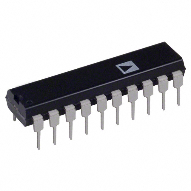
The AD7390/AD7391 are specified over the extended industrial (-40°C to +85°C) temperature range. The AD7391AR is specified for the -40°C to+125°C automotive temperature range. The AD7390/AD7391s are available in plastic DIP, and low profile 1.75 mm height SO-8 surface mount packages. The AD7391ARU is available for ultracompact applications in a thin 1.1 mm TSSOP-8 package.

 AD7391 Data Sheet


