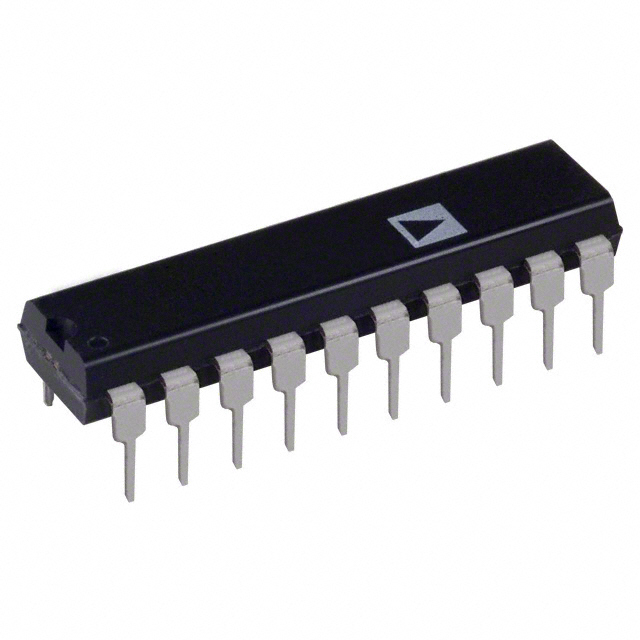
Features: Dual 12-bit SAR ADC Simultaneous samplingThroughput rate: 5 MSPS per channelSpecified for VDD at 2.5 V No conversion latencyPower dissipation: 36 mW at 5 MSPSOn-chip reference: 2.048 V ± 0.25%, 6 ppm/°CDual conversion with read High speed serial interface: SPI-/QSPI™-/MICROWIRET...
AD7356: Features: Dual 12-bit SAR ADC Simultaneous samplingThroughput rate: 5 MSPS per channelSpecified for VDD at 2.5 V No conversion latencyPower dissipation: 36 mW at 5 MSPSOn-chip reference: 2.048 V ± 0...
SeekIC Buyer Protection PLUS - newly updated for 2013!
268 Transactions
All payment methods are secure and covered by SeekIC Buyer Protection PLUS.
Resolution (Bits) | 12bit |
T-Put Rate | 5MSPS |
# Chan | 2 |
Supply V | Multi(+2.5, +3),Multi(+2.5, +3.3),Single(+2.5) |
Pwr Diss (max) | 59mW |
Interface | Ser,SPI |
Ain Range | (Vref) p-p,2.048 V p-p |
SNR (dB) | 71.5dB |
Pkg Type | SOP |
Parameter | Rating |
VDD to AGND, DGND, REFGND VDRIVE to AGND, DGND, REFGND VDD to VDRIVE AGND to DGND to REFGND Analog Input Voltages1 to AGND Digital Input Voltages2 to DGND Digital Output Voltages3 to DGND Input Current to Any Pin Except Supply Pins4 Operating Temperature Range Y Grade B Grade Storage Temperature Range Junction Temperature TSSOP JA Thermal Impedance JC Thermal Impedance Lead Temperature, Soldering Reflow Temperature (10 sec to 30 sec) ESD |
−0.3 V to +3 V −0.3 V to +5 V −5 V to +3 V −0.3 V to +0.3 V −0.3 V to VDD + 0.3 V −0.3 V to VDRIVE + 0.3 −0.3 V to VDRIVE + 0.3 ±10 mA −40 to +125 −40 to +85 −65 to +150 150 143/W 45/W 255 1.5 kV |
The AD73561 is a dual, 12-bit, high speed, low power, successive approximation ADC that operates from a single 2.5 V power supply and features throughput rates up to 5 MSPS. The part contains two ADCs, each preceded by a low noise, wide band- width track-and-hold circuit that can handle input frequencies in excess of 110 MHz. The conversion process and data acquisition use standard control inputs allowing for easy interfacing to microprocessors or DSPs. The input signal is sampled on the falling edge of CS; a conversion is also initiated at this point. The conversion time is etermined by the SCLK frequency. The AD7356 uses advanced design techniques to achieve very low power issipation at high throughput rates. With a 2.5 V supply and a 5 MSPS throughput rate, the part consumes typically 14 mA. The part also offers a flexible ower/throughput rate management option. The analog input range for the part is the differential common mode ±VREF/2. The AD7356 has an on-chip 2.048 V reference that can be overdriven when an external reference is preferred. The AD7356 is available in a 16-lead thin shrink small outline package (TSSOP).