AD7010

Features: Single +5 V SupplyOn-Chip p/4 DQPSK ModulatorRoot-Raised-Cosine Tx Filters, a = 0.5Two 10-Bit D/A Converters4th Order Reconstruction FiltersDifferential Analog OutputsOn-Chip Ramp Up/Down Power ControlOn-Chip Tx Offset CalibrationVery Low Power Dissipation, 30 mW typPower Down Mode < ...

product image

AD7010 Picture
SeekIC No. : 004269843 Detail

AD7010: Features: Single +5 V SupplyOn-Chip p/4 DQPSK ModulatorRoot-Raised-Cosine Tx Filters, a = 0.5Two 10-Bit D/A Converters4th Order Reconstruction FiltersDifferential Analog OutputsOn-Chip Ramp Up/Down ...

floor Price/Ceiling Price

Part Number:
AD7010
Supply Ability:
5000

Price Break

  • Qty
  • 1~5000
  • Unit Price
  • Negotiable
  • Processing time
  • 15 Days
Total Cost: $ 0.00

SeekIC Buyer Protection PLUS - newly updated for 2013!

  • Escrow Protection.
  • Guaranteed refunds.
  • Secure payments.
  • Learn more >>

Month Sales

268 Transactions

Rating

evaluate  (4.8 stars)

Upload time: 2024/11/21

Payment Methods

All payment methods are secure and covered by SeekIC Buyer Protection PLUS.

Notice: When you place an order, your payment is made to SeekIC and not to your seller. SeekIC only pays the seller after confirming you have received your order. We will also never share your payment details with your seller.
Product Details

Description


Features:

Single +5 V Supply
On-Chip p/4 DQPSK Modulator
Root-Raised-Cosine Tx Filters, a = 0.5
Two 10-Bit D/A Converters
4th Order Reconstruction Filters
Differential Analog Outputs
On-Chip Ramp Up/Down Power Control
On-Chip Tx Offset Calibration
Very Low Power Dissipation, 30 mW typ
Power Down Mode < 5 mA
On-Chip Voltage Reference
24-Pin SSOP


Application

Japanese Digital Cellular Telephony


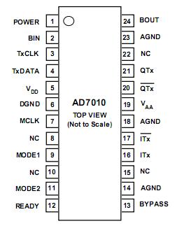
Pinout

  Connection Diagram


Specifications

VDD Tx, VDD Rx to AGND  . . . . . . . . . . . . . . . 0.3 V to +7 V
AGND to DGND  . . . . . . . . . . . . . . . . . . . . . 0.3 V to +0.3 V
Digital I/O Voltage to DGND  . . . . . 0.3 V to VDD to + 0.3 V
Analog I/O Voltage to AGND  . . . . . . .0.3 V to VDD + 0.3 V
Operating Temperature Range
Industrial (A Version)  . . . . . . . . . . . . . . . . 40°C to +85°C
Storage Temperature Range  . . . . . . . . . .65°C to +150°C
Junction Temperature  . . . . . . . . . . . . . . . . . . . . . . .+150°C
SSOP JA Thermal Impedance  . . . . . . . . . . . . . . +122°C/W
Lead Temperature, Soldering
Vapor Phase (60 sec)  . . . . . . . . . . . . . . . . . . . . .    +215°C
Infrared (15 sec)  . . . . . . . . . . . . . . . . . . . . . . . . .   +220°C


Description

The AD7010 is a complete low power, CMOS, /4 DQPSK modulator with single +5 V power supply. The part is designed to perform the baseband conversion of I and Q transmit waveforms in accordance with the Japanese Digital Cellular Telephone system. The on-chip /4 Differential Quadrature Phase Shift Keying (DQPSK) digital modulator, which includes the Root Raised Cosine filters, generates I and Q data in response to the transmit data stream. The AD7010 also contains ramp control envelope logic to shape the I and Q output waveforms when ramping up or down at the beginning or end of a transmit burst.

Besides providing all the necessary logic to perform /4 DQPSK modulation, the part also provides reconstruction filters to smooth the DAC outputs, providing continuous time analog outputs. The AD7010 generates differential analog outputs for both the I and Q signals. As it is a necessity for all digital mobile systems to use the lowest possible power, the device has power down options. The AD7010 is housed in a space efficient 24-pin SSOP (Shrink Small Outline Package).


Customers Who Bought This Item Also Bought

Margin,quality,low-cost products with low minimum orders. Secure your online payments with SeekIC Buyer Protection.
Cables, Wires
Optical Inspection Equipment
RF and RFID
Cables, Wires - Management
Discrete Semiconductor Products
Batteries, Chargers, Holders
View more