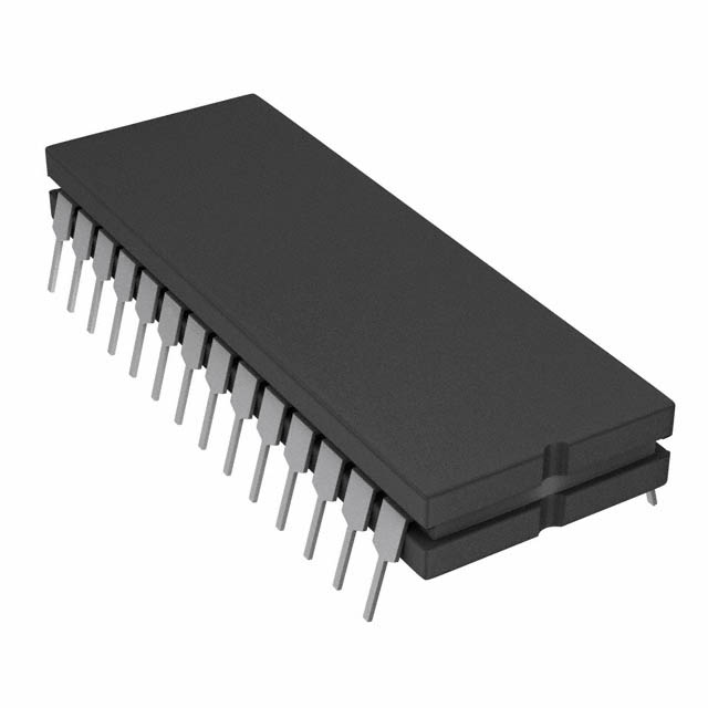
Series: -
Number of Converters: 2
Number of Bits: 12
Packaging: Tube
Sampling Rate (Per Second): 1.25M
Mounting Type: Through Hole
Operating Temperature: 0°C ~ 70°C
Data Interface: Parallel
Voltage Supply Source: Analog and Digital, Dual ±
Manufacturer: Analog Devices Inc
Supplier Device Package: 28-CDIP
Package / Case: 28-CDIP (0.600", 15.24mm)
Power Dissipation (Max): 750mW
Number of Inputs and Type: 2 Single-Ended, Bipolar; 2 Single-Ended, Unipolar
Pinout Description
The AD1671JQ is designed as a monolithic 12-bit, 1.25 MSPS analog-todigital converter with an on-board, high performance sampleand-hold amplifier (SHA) and voltage reference. It guarantees no missing codes over the full operating temperature range. The combination of a merged high speed bipolar/CMOS process and a novel architecture results in a combination of speed and power consumption far superior to previously available hybrid implementations.
AD1671JQ has ten features. (1) Conversion time: 800ns. (2) 1.25MHz throughput rate. (3) Complete: on-chip sample-and-hold amplifier and voltage reference. (4) Low power dissipation: 570mW. (5) No missing codes guaranteed. (6) Signal-to-noise plus distortion ratio fIN = 100kHz: 70dB. (7) Pin configurable input voltage ranges. (8) Twos complement or offset binary output data. (9) 28-pin DIP and 28-pin surface mount package. (10) Out of range indicator. That are all the main features.
Some absolute maximum ratings of AD1671JQ have been concluded into several points as follow. (1) Its Vcc would be from -0.5 to +6.5V. (2) Its Vee would be from -6.5 to +0.5V. (3) Its Vlogic would be from -0.5 to +6.5V. (4) Its ACOM with respect to DCOM would be from -1.0 to +1.0V. (5) Its Vcc with respect to Vlogic would be from -6.5 mto +6.5V. (6) Its ENCODE with respect to DCOM would be from -0.5V to Vlogic + 0.5V. (7) Its REF IN with respect to ACOM would be from -0.5 to Vc + 0.5V. (8) Its AIN would be from -11.0V to +11.0V. (9) Its BPO/UPO with respect to ACOM would be from -0.5 to Vcc + 0.5Volts. (10) Its junction temperature would be +150°C. (11) Its storage temperature would be from -65 to +150°C. (12) Its lead temperature (10 sec) would be +300°C. It should be noted that stresses above those listed under "absolute maximum ratings" may cause permanent damage to the device. And so on. If you have any question or suggestion or want to know more information please contact us for details. Thank you!
Parameters: | Technical/Catalog Information | AD1671JQ |
| Vendor | Analog Devices Inc |
| Category | Integrated Circuits (ICs) |
| Number of Bits | 12 |
| Package / Case | 28-CDIP (600 mil) |
| Data Interface | Parallel |
| Packaging | Tube |
| Sampling Rate (Per Second) | 1.25M |
| Operating Temperature | 0°C ~ 70°C |
| Voltage Supply Source | Analog and Digital, Dual ± |
| Number of Inputs and Type | 2 Single-Ended, Bipolar; 2 Single-Ended, Unipolar |
| Number of Converters | 2 |
| Power Dissipation (Max) | 750mW |
| Drawing Number | * |
| RoHS Status | RoHS Non-Compliant |
| Other Names | AD1671JQ
AD1671JQ
|

 AD1671JQ Data Sheet


