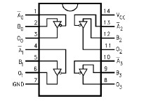
Features: High Speed: tPD=3.8 ns (typ) at VCC=5VLower power dissipation: ICC=4 A (max) at TA=25qCHigh noise immunity: VNIH=VNIL=28% VCC (min)Power down protection is provided on all inputsLow noise: VOLP=0.8V (max)Pin and function compatible with 74HC125PinoutSpecifications Supply Voltage (VC...
74VHC125: Features: High Speed: tPD=3.8 ns (typ) at VCC=5VLower power dissipation: ICC=4 A (max) at TA=25qCHigh noise immunity: VNIH=VNIL=28% VCC (min)Power down protection is provided on all inputsLow noise:...
SeekIC Buyer Protection PLUS - newly updated for 2013!
268 Transactions
All payment methods are secure and covered by SeekIC Buyer Protection PLUS.
Supply Voltage (VCC) | -0.5V to +7.0V |
DC Input Voltage (VIN) | -0.5V to +7.0V |
DC Output Voltage (VOUT) | -0.5V to VCC + 0.5V |
Input Diode Current (IIK) | -20 mA |
Output Diode Current (IOK) | ±20 mA |
DC Output Current (IOUT) | ±25 mA |
DC VCC/GND Current (ICC) | ±50 mA |
Storage Temperature (TSTG) | -65 to +150 |
Lead Temperature (TL) | |
(Soldering, 10 seconds) | 260 |
The 74VHC125 contains four independent non-inverting buffers with 3-STATE outputs. It is an advanced high-speed CMOS device fabricated with silicon gate CMOS technology and achieves the high-speed operation similar to equivalent Bipolar Schottky TTL while maintaining the CMOS low power dissipation.
An input protection circuit of the 74VHC125 insures that 0V to 7V can be applied to the input pins without regard to the supply voltage.This device can be used to interface 5V to 3V systems and two supply systems such as battery backup. This circuit prevents device destruction due to mismatched supply and input voltages.