Output Type
:
Low Level Output Current
:
Supply Voltage - Max
: 3.6 V
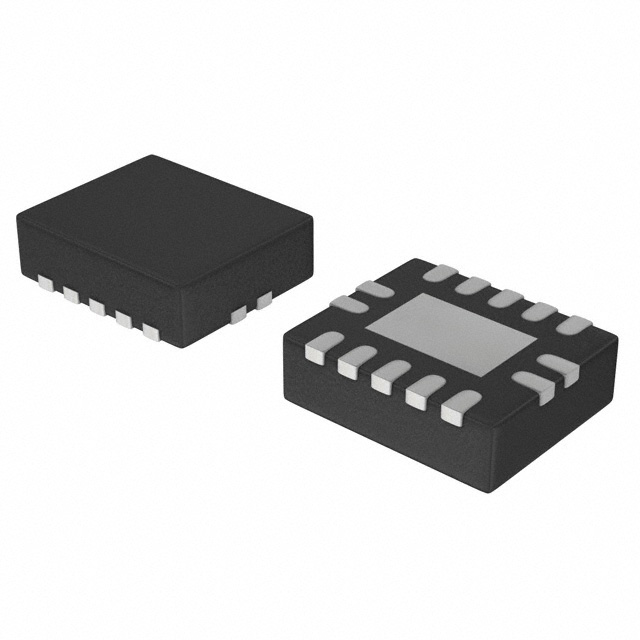
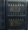
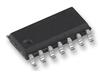
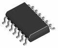
Mounting Style
: SMD/SMT
Number of Circuits
: 2
Input Type
: Single-Ended
Maximum Operating Temperature
: + 85 C
Packaging
: Tube
Polarity
: Inverting/Non-Inverting
Logic Type
: D-Type Edge Triggered Flip-Flop
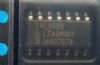
Logic Family
: LVT
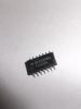
Package / Case
: SOT-108
Propagation Delay Time
: 3.6 ns at 3.3 V
High Level Output Current
: - 20 mA
DescriptionThe 74LVT74D belongs to the 74LVT74 family which is a dual positive edge-triggered D-type flip-flop featuring individual data, clock, set, and reset inputs; also true and complementary outputs. Data must be stable just one setup time prior to the low-to-high transition of the clock for predictable operation. Clock triggering occurs at a voltage level and is not directly related to the transition time of the positive-going pulse. Set (SD) and reset (RD) are asynchronous active low inputs and operate independently of the clock input. When set and reset are inactive (high), data at the D input is transferred to the Q and Q' outputs on the low-to-high transition of the clock. Following the hold time interval, data at the D input may be changed without affecting the levels of the output.
Some quick rederence data of 74LVT74D can be summarized as (1)tPLH, tPHL Propagation delay An to Yn(CL = 50pF)/(VCC = 3.3V): 3.1/3.6ns; (2)CIN input capacitance(VI = 0V or 3.0V): 3 pF; (3)ICCL total supply current(outputs low; VCC = 3.6V): 0.5mA.
The absolute maximum ratings of 74LVT74D are (1)VCC DC supply voltage: -0.5 to +4.6 V; (2)IIK DC input diode current (VI < 0): -50 mA; (3)VI DC input voltage3: -0.5 to +7.0 V; (4)IOK DC output diode current(VO < 0): -50 mA; (5)VOUT DC output voltage3(output in off or high state): -0.5 to +7.0V; (6)IOUT DC output current(output in low state/output in high state): 64/-32mA; (7)Tstg storage temperature range: -65 to 150 °C.(1. Stresses beyond those listed may cause permanent damage to the device. These are stress ratings only and functional operation of the device at these or any other conditions beyond those indicated under "recommended operating conditions" is not implied. Exposure to absolute-maximum-rated conditions for extended periods may affect device reliability. 2. The performance capability of a high-performance integrated circuit in conjunction with its thermal environment can create junction temperatures which are detrimental to reliability. The maximum junction temperature of this integrated circuit should not exceed 150°C. 3. The input and output negative voltage ratings may be exceeded if the input and output clamp current ratings are observed.).
 74LVT74D Data Sheet