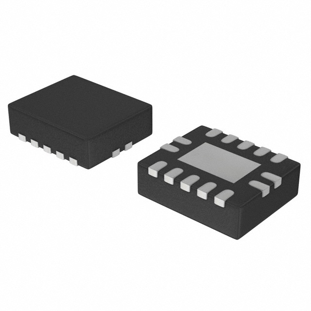
Features: • Independent registers for A and B buses• Multiplexed real-time and stored data• 3-State outputs• Output capability: +64mA/32mA• TTL input and output switching levels• Input and output interface capability to systems at 5V supply• Bus-hold data ...
74LVT652: Features: • Independent registers for A and B buses• Multiplexed real-time and stored data• 3-State outputs• Output capability: +64mA/32mA• TTL input and output switchi...
SeekIC Buyer Protection PLUS - newly updated for 2013!
268 Transactions
All payment methods are secure and covered by SeekIC Buyer Protection PLUS.
SYMBOL | PARAMETER |
CONDITIONS |
RATING |
UNIT |
VCC | DC supply voltage |
0.5 to +4.6 |
V | |
IIK | DC input diode current |
VI < 0 |
50 |
mA |
VI | DC input voltage3 |
0.5 to +7.0 |
V | |
IOK | DC output diode current |
VO < 0 |
50 |
mA |
VOUT | DC output voltage3 |
Output in Off |
0.5 to +7.0 |
V |
IOUT | DC output current |
Output in Low state Output in High state |
128 64 |
mA |
Tstg | Storage temperature range |
65 to +150 |
°C |
NOTES:
1. Stresses beyond those listed may cause permanent damage to the device. These are stress ratings only and functional operation of the device at these or any other conditions beyond those indicated under "recommended operating conditions" is not implied. Exposure to absolute-maximum-rated conditions for extended periods may affect device reliability.
2. The performance capability of a high-performance integrated circuit in conjunction with its thermal environment can create junction temperatures which are detrimental to reliability. The maximum junction temperature of this integrated circuit should not exceed 150°C.
3. The input and output negative voltage ratings may be exceeded if the input and output clamp current ratings are observed.
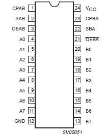
The 74LVT652 is a high-performance BiCMOS product designed for VCC operation at 3.3V.
This 74LVT652 combines low static and dynamic power dissipation with high speed and high output drive. The 74LVT652 transceiver/register consists of bus transceiver circuits with 3-State outputs, Dtype flip-flops, and control circuitry arranged for multiplexed transmission of data directly from the input bus or the internal registers. Data on the A or B bus will be clocked into the registers as the appropriate clock pin goes High. Output Enable (OEAB, OEBA) and Select (SAB, SBA) pins are provided for bus management.