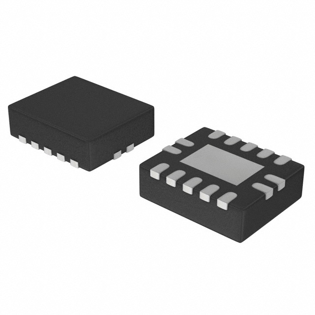
Features: • 18-bit bidirectional bus interface
• 3-State buffers
• Output capability: +64mA/-32mA
• TTL input and output switching levels
• Input and output interface capability to systems at 5V supply
• Bus-hold data inputs eliminate the need for external pull-up resistors to hold unused inputs
• Live insertion/extraction permitted
• Power-up reset
• Power-up 3-State
• No bus current loading when output is tied to 5V bus
• Negative edge-triggered clock inputs
• Latch-up protection exceeds 500mA per JEDEC JC40.2 Std 17
• ESD protection exceeds 2000V per MIL STD 883 Method 3015 and 200V per Machine Model
Pinout Specifications
|
SYMBOL |
PARAMETER |
CONDITIONS |
RATING |
UNIT |
|
VCC |
DC supply voltage |
|
0.5 to +4.6 |
V |
|
IIK |
DC input diode current |
VI < 0 |
50 |
mA |
|
VI |
DC input voltage3 |
|
0.5 to +7.0 |
V |
|
IOK |
DC output diode current |
VO < 0 |
50 |
mA |
|
VOUT |
DC output voltage3 |
Output in Off or High state |
0.5 to +7.0 |
V |
|
IOUT |
DC output current |
Output in High state |
32 |
mA |
|
Output in Low state |
64 |
|
Tstg |
Storage temperature range |
|
65 to 150 |
°C |
DescriptionThe 74LVT16500A is designed as a high-performance BiCMOS product designed for Vcc operation at 3.3V. This device is an 18-bit universal transceiver featuring non-inverting 3-State bus compatible outputs in both send and receive directions. Data flow in each direction is controlled by output enable, latch enable, and clock inputs.
The 74LVT16500A has many features. The first one is 18-bit bidirectional bus interface. The second one is 3-State buffers. The third one is output capability is +64mA/-32mA. The fourth one is TTL input and output switching levels. The fifth one is input and output interface capability to systems at 5V supply. The sixth one is bus-hold data inputs eliminate the need for external pull-up resistors to hold unused inputs. The seventh one is live insertion/extraction permitted. The eighth one is power-up reset. The ninth one is power-up 3-state. The tenth one is no bus current loading when output is tied to 5V bus. The eleventh one is negative edge triggered clock inputs. The twelfth one is latch-up protection exceeds 500mA per JEDEC JC40.2 Std 17. The thirteenth one is ESD protection exceeds 2000V per MIL-STD-883 method 3015 and 200V per machine model. That are all the main features.
Some absolute maximum ratings of the 74LVT16500A have been concluded into several points as follow. The first one is about its DC supply voltage which would be from 0.5 to +4.6V. The second one is about its DC input diode current which would be 50mA. The third one is about its DC input voltage which would be from 0.5 to +7.0V. The fourth one is about its DC output diode current which would be 50mA. The fifth one is about its DC output voltage which would be from -0.5 to +7.0V. The sixth one is about its DC output current which would be 128mA for low state and would be -64mA for high state. The seventh one is about its storage temperature range which would be from 65 to +150°C. It should be noted that stresses beyond those listed may cause permanent damage to the device. And so on. For more information please contact us.
The 74LVT16500A is a high-performance BiCMOS product designed for VCC operation at 3.3V.
This device is an 18-bit universal transceiver featuring non-inverting 3-State bus compatible outputs in both send and receive directions. Data flow in each direction is controlled by output enable (OEAB and OEBA), latch enable (LEAB and LEBA), and clock (CPAB andCPBA) inputs. For A-to-B data flow, the device operates in the transparent mode when LEAB is High. When LEAB is Low, the A data is latched if CPAB is held at a High or Low logic level. If LEAB is Low, the A-bus data is stored in the latch/flip-flop on the High-to-Low transition of CPAB. When OEAB is High, the outputs are active. When OEAB is Low, the outputs are in the high-impedance state.
Data flow for B-to-A is similar to that of A-to-B but uses OEBA, LEBA and CPBA. The output enables are complimentary (OEAB is active High, and OEBA is active Low).
Active bus-hold circuitry is provided to hold unused or floating data inputs at a valid logic level.

 74LVT16500A Data Sheet


