DescriptionThe 74LVT126D belongs to LVT126 is a high-performance BiCMOS product designed for VCC operation at 3.3V. This device combines low static and dynamic power dissipation with high speed and high output drive. The 74LVT126 device is a quad buffer that is ideal for driving bus lines. The dev...
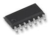
74LVT126D: DescriptionThe 74LVT126D belongs to LVT126 is a high-performance BiCMOS product designed for VCC operation at 3.3V. This device combines low static and dynamic power dissipation with high speed and ...
SeekIC Buyer Protection PLUS - newly updated for 2013!
268 Transactions
All payment methods are secure and covered by SeekIC Buyer Protection PLUS.
The 74LVT126D belongs to LVT126 is a high-performance BiCMOS product designed for VCC operation at 3.3V. This device combines low static and dynamic power dissipation with high speed and high output drive. The 74LVT126 device is a quad buffer that is ideal for driving bus lines. The device features four Output Enables (OE0, OE1, OE2, OE3), each controlling one of the 3-State outputs.
The features of 74LVT126D can be summarized as (1)quad bus interface; (2)3-state buffers; (3)output capability: +64mA/-32mA; (4)TTL input and output switching levels; (5)input and output interface capability to systems at 5V supply; (6)bus-hold data inputs eliminate the need for external pull-up resistors to hold unused inputs; (7)live insertion/extraction permitted; (8)no bus current loading when output is tied to 5V bus; (9)power-up 3-State; (10)latch-up protection exceeds 500mA per JEDEC Std 17; (11)ESD protection exceeds 2000V per MIL STD 883 Method 3015 and 200V per machine model.
The absolute maximum ratings of 74LVT126D are (1)VCC DC supply voltage: -0.5 to +4.6 V; (2)VI DC input voltage3: -0.5 to +7.0 V; (3)VOUT DC output voltage3(output in off or high state): -0.5 to +7.0 V; (4)IOUT DC output current(output in low state/out in high state): 128 mA/-64 mA; (5)IIK DC input diode current VI < 0: -50 mA; (6)IOK DC output diode current VO < 0: -50 mA; (7)Tstg Storage temperature range: -65 to 150 °C.(1. Stresses beyond those listed may cause permanent damage to the device. These are stress ratings only and functional operation of the device at these or any other conditions beyond those indicated under "recommended operating conditions" is not implied. Exposure to absolute-maximum-rated conditions for extended periods may affect device reliability. 2. The performance capability of a high-performance integrated circuit in conjunction with its thermal environment can create junction temperatures which are detrimental to reliability. The maximum junction temperature of this integrated circuit should not exceed 150°C. 3. The input and output negative voltage ratings may be exceeded if the input and output clamp current ratings are observed.).