74LVQ74

Features: ` Ideal for low power/low noise 3.3V applications` Guaranteed simultaneous switching noise level and dynamic threshold performance` Guaranteed pin-to-pin skew AC performance` Guaranteed incident wave switching into 75PinoutSpecificationsSupply Voltage (VCC) . . . . . . . .. . . . . . . ....

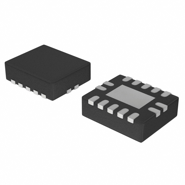
product image

74LVQ74 Picture
SeekIC No. : 004251468 Detail

74LVQ74: Features: ` Ideal for low power/low noise 3.3V applications` Guaranteed simultaneous switching noise level and dynamic threshold performance` Guaranteed pin-to-pin skew AC performance` Guaranteed in...

floor Price/Ceiling Price

Part Number:
74LVQ74
Supply Ability:
5000

Price Break

  • Qty
  • 1~5000
  • Unit Price
  • Negotiable
  • Processing time
  • 15 Days
Total Cost: $ 0.00

SeekIC Buyer Protection PLUS - newly updated for 2013!

  • Escrow Protection.
  • Guaranteed refunds.
  • Secure payments.
  • Learn more >>

Month Sales

268 Transactions

Rating

evaluate  (4.8 stars)

Upload time: 2024/11/23

Payment Methods

All payment methods are secure and covered by SeekIC Buyer Protection PLUS.

Notice: When you place an order, your payment is made to SeekIC and not to your seller. SeekIC only pays the seller after confirming you have received your order. We will also never share your payment details with your seller.
Product Details

Description


Features:

` Ideal for low power/low noise 3.3V applications
` Guaranteed simultaneous switching noise level and dynamic threshold performance
` Guaranteed pin-to-pin skew AC performance
` Guaranteed incident wave switching into 75


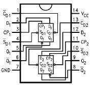
Pinout

  Connection Diagram


Specifications

Supply Voltage (VCC) . . . . . . . . . . . . . . . .  . . . . . . . .  . . . . . . . .  . . . . .  . . . . .   . .  −0.5V to +7.0V
DC Input Diode Current (IIK)
   VI = −0.5V  . . . . . . . .  . . . . . . . .  . . . . . . . .  . . . . . . . .  . . . . . . . .  . . . . . . . .. . . . . . . . . . −20 mA
   VI = VCC + 0.5V  . . . . . . . .  . . . . . . . .  . . . . . . . .  . . . . . . . .  . . . . . . . .   . . . .  . . . . . . . . +20 mA
DC Input Voltage (VI)  . . . . . . . .  . . . . . . . .  . . . . . . . .  . . . . . . . .  . . . . .  .. . . −0.5V to VCC + 0.5V
DC Output Diode Current (IOK)
   VO = −0.5V  . . . . . . . .  . . . . . . . .  . . . . . . . .  . . . . . . . .  . . . . . . . .  . . . . . . .  .  . . . . . . . . −20 mA
   VO = VCC + 0.5V  . . . . . . . .  . . . . . . . .  . . . . . . . .  . . . . . . . .  . . . . . . . .  . . . . . .. . . . . . . +20 mA
DC Output Voltage (VO)  . . . . . . . .  . . . . . . . .  . . . . . . . .  . . . . . . . .  . . . . . . . −0.5V to VCC + 0.5V
DC Output Source
   or Sink Current (IO)  . . . . . . . .  . . . . . . . .  . . . . . . . .  . . . . . . . .  . . . . . . . .  . . . . . . . . . . ±50 mA
DC VCC or Ground Current
   (ICC or IGND)  . . . . . . . .  . . . . . . . .  . . . . . . . .  . . . . . . . .  . . . . . . . .  . . . . . . . . . . .   . . ±200 mA
Storage Temperature (TSTG)  . . . . . . . .  . . . . . . . .  . . . . . . . .  . . . . . . . . . . . . . −65°C to +150°C
DC Latch-Up Source or
   Sink Current  . . . . . . . .  . . . . . . . .  . . . . . . . .  . . . . . . . .  . . . . . . . .  . . . . . . . .  . .. . . . . ±100 mA
Supply Voltage (VCC)  . . . . .  . . . . . . . . . . .  . . . . . . . . . . .  . . . . . . . . . . .  . . . . . . . . . . 2.0V to 3.6V
Input Voltage (VI) . . . . .  . . . . . . . . . . .  . . . . . . . . . . .  . . . . . . . . . . .  . . . . . . . . . . . . . . . 0V to VCC
Output Voltage (VO)  . . . . .  . . . . . . . . . . .  . . . . . . . . . . .  . . . . . . . . . . .  . . . . . ..  . . . . . .0V to VCC
Operating Temperature (TA)  . . . . .  . . . . . . . . . . .  . . . . . . . . . . .  . . . . . . . . . . . .−40°C to +85°C
Minimum Input Edge Rate (V/t)
   VIN from 0.8V to 2.0V
   VCC @ 3.0V  . . . . .  . . . . . . . . . . .  . . . . . . . . . . .  . . . . . . . . . . .  . . . . . . . . . . .  . . . . . . 125 mV/ns

Note 1: The "Absolute Maximum Ratings" are those values beyond which the safety of the device cannot be guaranteed. The device should not be operated at these limits. The parametric values defined in the Electrical Characteristics tables are not guaranteed at the absolute maximum ratings. The "Recommended Operating Conditions" table will define the conditions for actual device operation.
Note 2: Unused inputs must be held HIGH or LOW. They may not float.


Description

The 74LVQ74 is a dual D-type flip-flop with Asynchronous Clear and Set inputs and complementary (Q, Q) outputs. Information at the input is transferred to the outputs on the positive edge of the clock pulse. Clock triggering occurs at a voltage level of the clock pulse and is not directly related to the transition time of the positive-going pulse. After the Clock Pulse input threshold voltage has been passed, the Data input is locked out and information present will not be transferred to the outputs until the next rising edge of the Clock Pulse input.

Asynchronous Inputs of the 74LVQ74:
   LOW input to SD (Set) sets Q to HIGH level
   LOW input to CD (Clear) sets Q to LOW level
   Clear and Set are independent of clock
   Simultaneous LOW on CD and SD makes both
   Q and Q HIGH


Customers Who Bought This Item Also Bought

Margin,quality,low-cost products with low minimum orders. Secure your online payments with SeekIC Buyer Protection.
Optical Inspection Equipment
LED Products
Optoelectronics
Test Equipment
Prototyping Products
DE1
View more