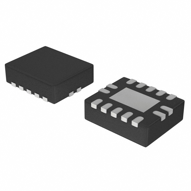
Features: ·HIGHSPEED: fMAX = 150MHz(TYP.) at VCC =3.3V·COMPATIBLEWITH TTL OUTPUTS· LOWPOWERDISSIPATION: ICC =4 mA (MAX.) at TA =25 oC·LOWNOISE: VOLP = 0.3 V (TYP.) at VCC = 3.3V· 75W TRANSMISSIONLINEDRIVING CAPABILITY·SYMMETRICAL OUTPUT IMPEDANCE: |IOH| = IOL = 12mA (MIN)· PCI BUSLEVELSGUARANTEED ...
74LVQ174: Features: ·HIGHSPEED: fMAX = 150MHz(TYP.) at VCC =3.3V·COMPATIBLEWITH TTL OUTPUTS· LOWPOWERDISSIPATION: ICC =4 mA (MAX.) at TA =25 oC·LOWNOISE: VOLP = 0.3 V (TYP.) at VCC = 3.3V· 75W TRANSMISSIONLIN...
SeekIC Buyer Protection PLUS - newly updated for 2013!
268 Transactions
All payment methods are secure and covered by SeekIC Buyer Protection PLUS.
SYMBOL | PARAMETER | Value | UNIT |
VCC | Supply voltagee | 0.5 to+ 7 | V |
VI | DC Input Voltage | -0.5 to VCC + 0.5 | V |
VO | DC Output Voltage | -0.5 to VCC + 0.5 | V |
IIK | DC Input Diode Current | ± 20 | mA |
IOK | DC Output Diode Current | ± 20 | mA |
IO | DC Output Current | ± 50 | mA |
ICC or IGND | DC VCC or Ground Current | ± 200 | mA |
Tstg | Storage temperature | 65 to 150 | |
TL |
Lead Temperature (10 sec) | 300 |
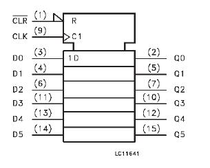
The 74LVQ174 is a low voltage CMOS HEX D-TYPE FLIP FLOP WITH CLEAR NON INVERTING fabricated with sub-micron silicon gate and double-layer metal wiring C2MOS technology. It is ideal for low power and low noise 3.3V applications.
Information signals applied to D inputs are transfered to the Q outputs on the positive going edge of the clock pulse.
When the CLEAR input of the 74LVQ174 is held low, the Q outputs are held low independentely of the other inputs .
It has better speed performance at 3.3V than 5V LS-TTL family combined with the true CMOS low power consumption.
All inputs and outputs of the 74LVQ174 are equipped with protection circuits against static discharge, giving them 2KV ESD immunity and transient excess voltage.