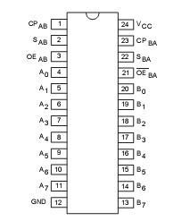
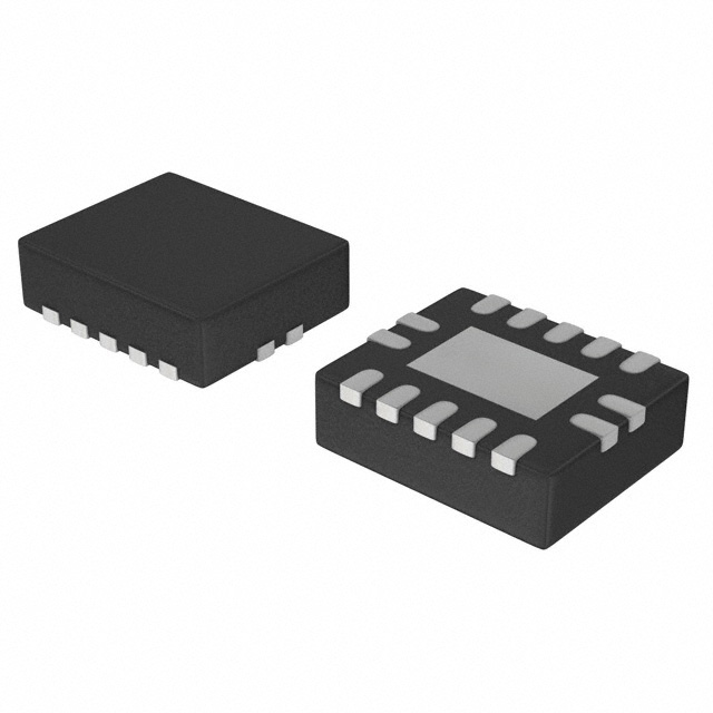
Features: Wide supply voltage range of 1.2V to 3.6V
In accordance with JEDEC standard no. 8-1A
CMOS low power consumption
Direct interface with TTL levels
5 Volt tolerant inputs/outputs, for interfacing with 5 Volt logicPinout Specifications
| |
PARAMETER
|
CONDITIONS
|
LIMITS |
UNIT
|
| MIN |
MAX |
| VCC |
DC supply voltage (for max. speed performance) |
|
2.7 |
3.6 |
V |
| DC supply voltage (for low-voltage applications) |
|
1.2 |
3.6 |
| VI |
DC input voltage range |
|
0 |
5.5 |
V |
| VI/O |
DC input voltage range for I/Os |
|
0 |
VCC |
V |
| VO |
DC output voltage range |
|
0 |
VCC |
V |
| Tamb |
Operating free-air temperature range |
|
-40 |
+85 |
|
tr, tf
|
Input rise and fall times |
VCC= 1.2 to 2.7V
VCC= 2.7 to 3.6V
|
0
0 |
20
10 |
ns/V |
Description The 74LVC652 is a high performance,low-power, low-voltage Si-gate CMOS device,superior to most advanced CMOS compatible TTL families.
Inputs can be driven from either 3.3V or 5.0V devices. In 3-State operation, outputs can handle 5V. This feature allows the use of these devices as translators in a mixed 3.3V/5V environment.
The 74LVC652 consist of 8 non-inverting bus transceiver circuits with 3-State outputs, D-type flip-flops and control circuitry arranged for multiplexed transmission of data directly from the internal registers. Data on the 'A' or 'B' or both buses, will be stored in the internal registers, at the appropriate clock inputs (CPAB or CPBA) regardless of the select inputs (SAB and SBA) or output enable (OEAB and OEBA) control inputs. Depending on the select inputs SAB and SBA data can directly go from input to output (real time mode) or data can be controlled by the clock (storage mode), this is when the OEn inputs this operating mode permits. The output enable inputs OEAB and OEBA determine the operation mode of the transceiver.
When OEAB is LOW, no data transmission from An to Bn is possible and when OEBA is HIGH, there is no data transmission from Bn to An possible. When SAB and SBA are in the real time transfer mode, it is also possible to store data without using the internal D-type flip-flops by simultaneously enabling OEAB and OEBA. In this configuration each output reinforces its input.

 74LVC652 Data Sheet


