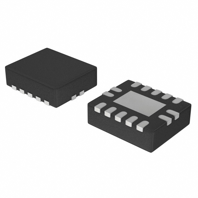
Features: Wide supply voltage range of 1.2V to 3.6V
Flow-through pin-out architecture
In accordance with JEDEC standard no. 8-1A
CMOS low power consumption
Direct interface with TTL levels
5 Volt tolerant inputs/outputs, for interfacing with 5 Volt logic
Pinout Specifications
| SYMBOL |
PARAMETER |
CONDITIONS |
RATING |
UNIT |
| VCC |
DC supply voltage |
|
0.5 to +6.5 |
V |
| IIK |
DC input diode current |
VI<0
|
50 |
mA |
| VI |
DC input voltage |
Note 2 |
0.5 to +6.5 |
V |
| IOK |
DC output diode current |
VO>VCC or V0< 0
|
50 |
mA |
VO
|
DC output voltage; output HIGH or LOW |
Note 2 |
0.5 to VCC+0.5 |
V |
| DC output voltage; output 3-State |
Note 2 |
0.5 to 6.5 |
mA |
| IO |
DC output diode current |
VO= 0 to VCC |
50 |
mA |
| IGND, ICC |
DC VCCor GND current |
|
100 |
V |
| Tstg |
Storage temperature range |
|
65 to +150 |
°C |
PTOT
|
Power dissipation per package
plastic mini-pack (SO)
plastic shrink mini-pack (SSOP and
TSSOP) |
above +70°C derate linearlywith 8 mW/K
above +60°C derate linearly with 5.5 mW/K |
500
500 |
mW |
DescriptionThe 74LVC646A is a high performance, low-power, low-voltage Si-gate CMOS device, superior to most advanced CMOS compatible TTL families.
Inputs can be driven from either 3.3V or 5.0V devices. In 3-State operation, outputs can handle 5V. This feature allows the use of these devices as translators in a mixed 3.3V/5V environment.
The 74LVC646A consist of non-inverting bus transceiver circuits with 3-State outputs, D-type flip-flops and control circuitry arrangedfor multiplexed transmission of data directly from the internal registers. Data on the 'A' or 'B' bus will be clocked in the internal registers, as the appropriate clock (CPAB or CPBA) goes to a HIGH logic level. Output enable (OE) and direction (DIR) inputs are provided to control the transceiver function. In the transceiver mode, data present at the high-impedance port may be stored in either the'A' or 'B' register, or in both. The select source inputs (SAB and SBA) can multiplex stored and real-time (transparent mode) data.
The direction (DIR) input of the 74LVC646A is which bus will receive data when OE is active (LOW). In the isolation mode (OE = HIGH), 'A'data may be stored in the 'B' register and/or 'B' data may be storedin the 'A' register.
When an output function of the 74LVC646A is disabled, the input function is still enabled and may be used to store and transmit data. Only one of the two buses, 'A' or 'B' may be driven at a time.
The '646A' is functionally identical to the '648A' but has non-inverting data paths.

 74LVC646A Data Sheet


