Features: •Wide supply voltage range of 1.2V to 3.6V
•In accordance with JEDEC standard no. 8-1A
•Flow-through pin-out architecture
•CMOS low power consumption
•Inputs accept voltages up to 5.5V
•Direct interface with TTL levels
•Output drive capability 50� transmission lines @ 85°C
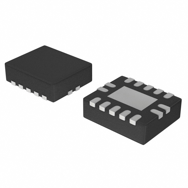
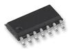
Pinout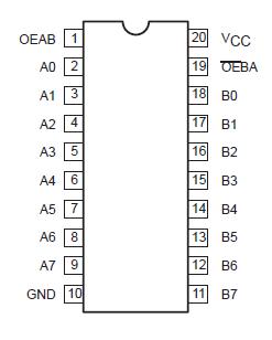 Specifications
| SYMBOL |
PARAMETER |
CONDITIONS |
RATING |
UNIT |
| VCC |
DC supply voltage |
|
0.5 to +6.5 |
V |
| IIK |
DC input diode current |
VI0 |
50 |
mA |
| VI |
DC input voltage |
Note 2 |
0.5 to +6.5 |
V |
| IOK |
DC output diode current |
VOVCC or VO0 |
±50 |
mA |
| VO |
DC output voltage; output HIGH or LOW state |
Note 2 |
0.5 to VCC+0.5 |
V |
| |
DC output voltage; output 3-State |
Note 2 |
0.5 to 6.5 |
|
| IO |
DC output source or sink current |
VO = 0 to VCC |
±50 |
mA |
| IGND,ICC |
DC VCC or GND current |
|
±100 |
mA |
| Tstg |
Storage temperature range |
|
65 to +150 |
|
| PTOT |
Power dissipation per package
plastic mini-pack (SO)
plastic shrink mini-pack (SSOP and TSSOP) |
above+70°Cderatelinearlywith8mW/K
above +60°C derate linearly with 5.5mW/K |
500
500 |
mW |
DescriptionThe 74LVC623A is a high performance, low-power, low-voltage Si-gate CMOS device, superior to most advanced CMOS compatible TTL families.
The 74LVC623A is an octal transceiver featuring non-inverting 3-State bus compatible outputs in both send and receive directions. This octal bus transceiver is designed for asynchronous two-way communication between data buses.
The control function implementation allows maximum flexibility in timing. This device allows data transmission from the A bus to the B bus or from the B bus to the A bus, depending upon the levels at the enable inputs (OE ~AB, OE BA). The enable inputs can be used to disable the device so that the buses are effectively isolated. The dual enable function configuration gives this transceiver the capability to store data by simultaneous enabling of OEAB and OE BA. Each output reinforces its input in this transceiver configuration. Thus, when both control inputs of the 74LVC623A are enabled and all other data sources to the two sets of the bus lines are at high impedance OFF-state, both sets of bus lines will remain at their last states. The 8-bit codes appearing on the two sets of buses will be identical.
The '623A' is identical to the '620A' but has true (non-inverting) outputs.

 74LVC623A Data Sheet