Polarity
: Non-Inverting
Mounting Style
: SMD/SMT
Maximum Operating Temperature
: + 125 C
Number of Input Lines
: 8
Number of Output Lines
: 8
Supply Voltage - Max
: 3.6 V
Supply Voltage - Min
: 1.2 V
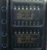
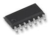
Packaging
: Tube
Package / Case
: SOT-163-20
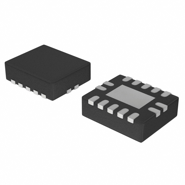
Pinout
 Description
The 74LVC541AD is a high-performance,low-power, low-voltage,Si-gate CMOS device,superior to most advanced CMOS compatible TTL families.The 74LVC541AD is an octal dual non-inverting buffer/line driver with 5-volt tolerant inputs/outputs.The 3-state outputs are controlled by the output enable inputs OE1 and OE2.
Features of the 74LVC541AD are:(1)5v tolerant inputs/outputs,for interfacing with 5-volt logic;(2)wide supply voltage range of 1.2V to 3.6V;(3)complles with JEDEC standard no.8-1A;(4)CMOS low power consumption;(5)direct interface with TTL levels.
The absolute maximum ratings of the 74LVC541AD can be summarized as:(1):the symbol is VCC,the parameter is supply voltage,the rating is -0.5 to +6.5,the unit is V;(2):the symbol is IIK,the parameter is DC input diode current,the rating is -50,the unit is mA;(3):the symbol is VI,the parameter is DC input voltage,the rating is -0.5 to +5.5,the unit is V;(4):the symbol is IOK,the parameter is DC output diode current,the rating is ±50,the unit is mA;(5):the symbol is VI/O,the parameter is DC output voltage:output high or low state,the rating is -0.5 to Vcc+0.5,the unit is V;(6):the symbol is VI/O,the parameter is DC output voltage:output 3-state,the rating is -0.5 to 6.5,the unit is V;(7):the symbol is IO,the parameter is DC output current source or sink current of the 74LVC541AD, the rating is ±50,the unit is mA;(8):the symbol is IGND,ICC,the parameter is DC VCC or GND current,the rating is ±100,the unit is mA;(9):the symbol is Tstg,the parameter is storage temperature range,the rating is -65 to +150,the unit is ;(10):the symbol is PTOT,the parameter power dissipation per package plastic mini-pack(SO),the rating is 500,the unit is mW;(11):the symbol is PTOT,the parameter power dissipation per package plastic shrink mini-pack(SSOP and TSSOP),the rating is 500,the unit is mW.
The 74LVC541AD octal buffer/line driver with 5-volt tolerant inputs/outputs (3-State). It is a high performance, low-power, low-voltage Si-gate CMOS device and superior to most advanced CMOS compatible TTL families. Besides, it is available in 20-Pin plastic SO package.
There are some features of the 74LVC541AD as follows: (1)5-volt tolerant inputs/outputs, for interfacing with 5-volt logic; (2)wide supply voltage range of 2.7V to 3.6V; (3)complies with JEDEC standard no. 8-1A; (4)CMOS low power consumption; (5)direct interface with TTL levels; (6)5 Volt tolerant inputs/outputs, for interfacing with 5 Volt logic.
What comes next is about the maximum ratings of the 74LVC541AD: (1)VCC, DC supply voltage: 0.5 to +6.5 V; (2)IIK, DC input diode current at VI<0: 50 mA; (3)VI, DC input voltage: 0.5 to +5.5 V; (4)IOK, DC output diode current at VO>VCC or VO<0: ±50 mA; (5)VO, DC output voltage (output HIGH or LOW): 0.5 to VCC+0.5 V; (6)VO, DC output voltage (output 3-State): 0.5 to +6.5 V; (7)IO, DC output diode current at VO=0 to VCC: ±50 mA; (8)IGND, ICC DC VCC or GND current: ±100 mA; (9)Tstg, storage temperature range of the 74LVC541AD: 60 to +150; (10)PTOT, power dissipation per package: 500 mW for plastic mini-pack (SO) package.

 74LVC541AD Data Sheet