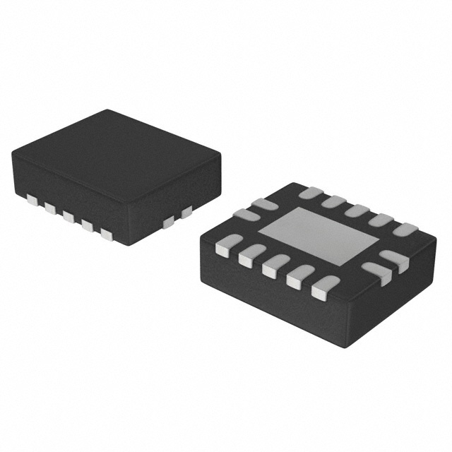
74LVC4066

Features: ` Very low ON resistance: 7.5 W (typical) at VCC = 2.7 V 6.5 W (typical) at VCC = 3.3 V 6W (typical) at VCC = 5 V.` ESD protection: HBM EIA/JESD22-A114-A Exceeds 2000 V MM EIA/JESD22-A115-A Exceeds 200 V.` High noise immunity` CMOS low power consumption` Latch up performance exceeds...

product image

74LVC4066 Picture
SeekIC No. : 004251353 Detail

74LVC4066: Features: ` Very low ON resistance: 7.5 W (typical) at VCC = 2.7 V 6.5 W (typical) at VCC = 3.3 V 6W (typical) at VCC = 5 V.` ESD protection: HBM EIA/JESD22-A114-A Exceeds 2000 V MM EIA/JESD22-...

floor Price/Ceiling Price

Part Number:
74LVC4066
Supply Ability:
5000

Price Break

  • Qty
  • 1~5000
  • Unit Price
  • Negotiable
  • Processing time
  • 15 Days
Total Cost: $ 0.00

SeekIC Buyer Protection PLUS - newly updated for 2013!

  • Escrow Protection.
  • Guaranteed refunds.
  • Secure payments.
  • Learn more >>

Month Sales

268 Transactions

Rating

evaluate  (4.8 stars)

Upload time: 2024/11/21

Payment Methods

All payment methods are secure and covered by SeekIC Buyer Protection PLUS.

Notice: When you place an order, your payment is made to SeekIC and not to your seller. SeekIC only pays the seller after confirming you have received your order. We will also never share your payment details with your seller.
Product Details

Description


Features:

` Very low ON resistance:
  7.5 W (typical) at VCC = 2.7 V
  6.5 W (typical) at VCC = 3.3 V
  6W (typical) at VCC = 5 V.
` ESD protection:
  HBM EIA/JESD22-A114-A Exceeds 2000 V
  MM EIA/JESD22-A115-A Exceeds 200 V.
` High noise immunity
` CMOS low power consumption
` Latch up performance exceeds 250 mA
` Complies with JEDEC standard no. 8-1A
` Direct interface TTL-levels.


Pinout

  Connection Diagram


Specifications

Symbol
Parameter
CONDITIONS
Min
Max
Unit
VCC
Supply Voltage
-0.5
+6.5
V
VI
input voltage
-0.5
+6.5
V
IIK
input diode current
VI < -0.5 V or VI > 6.5 V
-50
mA
ISK
switch diode current
VI < -0.5 V or VI > 6.5 V
±50
mA
VS
DC switch voltage range
enable and disable mode
-0.5
+6.5
V
IS
switch source or sink
current
VS < -0.5 V or VS > 6.5 V
±50
mA
ICC or IGND
VCC or Ground
±100
mA
Tstg
Storage temperature
-65
+150
PTOT
power dissipation
Tamb = -40 to +125 °C; note 3
300
mW
1. To avoid drawing VCC current out of terminal Z, when switch current flows in terminal Y, the voltage drop across the
bidirectional switch must not exceed 0.4 V. If the switch current flows into terminal Z, no VCC current will flow out of
terminal Y. In this case there is no limit for the voltage drop across the switch, but the voltage at Y and Z may not
exceed VCC or GND.
2. The input and output voltage ratings may be exceeded if the input and output current ratings are observed.
3. For SO14 packages: above 70 °C derate linearly with 8 mW/K.
For TSSOP14 packages: above 60 °C derate linearly with 5.5 mW/K.
For DHVQFN14 packages: above 60 °C derate linearly with 4.5 mW/K.


Description

The 74LVC4066 is a high-speed Si-gate CMOS device.

The 74LVC4066 has four independent analog switches. Each switch has two input/output terminals (nY and nZ) and an active HIGH enable input (nE). When nE is LOW,
the analog switch is turned off.


Customers Who Bought This Item Also Bought

Margin,quality,low-cost products with low minimum orders. Secure your online payments with SeekIC Buyer Protection.
Fans, Thermal Management
Prototyping Products
DE1
Batteries, Chargers, Holders
Soldering, Desoldering, Rework Products
Motors, Solenoids, Driver Boards/Modules
Isolators
View more