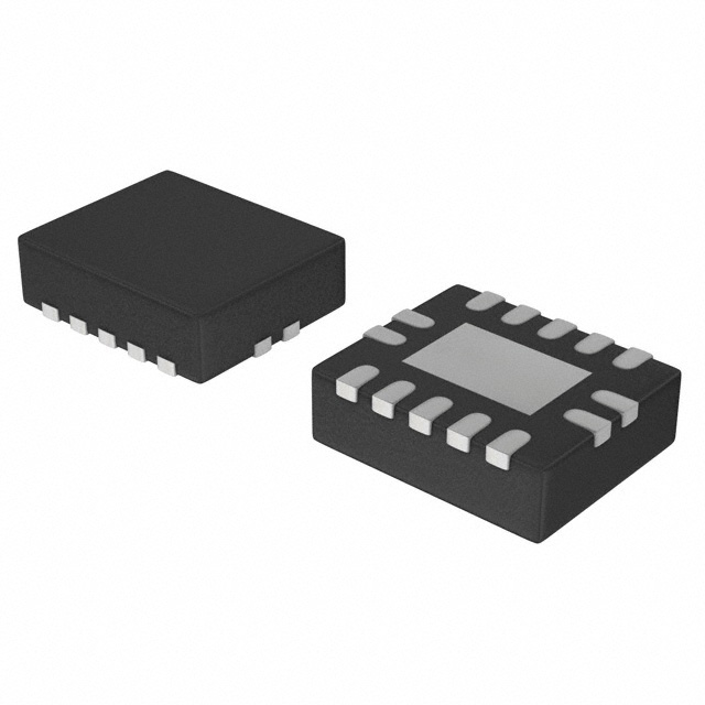
Features: • Wide supply voltage range from 1.65 to 5.5 V• 5 V tolerant input and a 5 V overvoltage tolerantpowered down output.• High noise immunity• Complies with JEDEC standard: JESD8-7 (1.65 to 1.95 V) JESD8-5 (2.3 to 2.7 V) JESD8B/JESD36 (2.7 to 3.6 V).•±24 mA out...
74LVC1GX04: Features: • Wide supply voltage range from 1.65 to 5.5 V• 5 V tolerant input and a 5 V overvoltage tolerantpowered down output.• High noise immunity• Complies with JEDEC stan...
SeekIC Buyer Protection PLUS - newly updated for 2013!
268 Transactions
All payment methods are secure and covered by SeekIC Buyer Protection PLUS.
SYMBOL |
PARAMETER |
CONDITIONS |
MIN. |
MAX. |
UNIT |
VCC |
supply voltage |
note 1 |
1.65 |
5.5 |
V |
VI |
input voltage |
5.5 |
V | ||
VO |
output voltage |
note 2 active mode Power-down mode; VCC = 0 V |
0 0 |
VCC 5.5 |
V V |
Tamb |
operating ambient temperature |
−40 |
+125 |
°C | |
tr, tf |
input rise and fall times |
VCC = 1.65 to 2.7 V |
0 |
20 |
ns/V |
VCC = 2.7 to 5.5 V |
0 |
10 |
ns/V |
The 74LVC1GX04 is a high-performance, low-power,low-voltage, Si-gate CMOS device and superior to mostadvanced CMOS compatible TTL families.Inputs can be driven from either 3.3 or 5 V devices. Thisfeature allows the use of this device as translator in amixed 3.3 and 5 V environment.This device is fully specified for partial power-downapplications using Ioff at output Y. The Ioff circuitry disablesthe output Y, preventing the damaging backflow currentthrough the device when it is powered down.
The 74LVC1GX04 combines the functions of the74LVC1GU04 and 74LVC1G04 to provide a deviceoptimized for use in crystal oscillator applications.The integration of the two devices into the 74LVC1GX04produces the benefits of a compact footprint, lower powerdissipation and stable operation over a wide range offrequency and temperature.