PinoutDescriptionThe 74LVC1G384GW is one member of the 74LVC1G384 family which is designed as the high-speed Si-gate CMOS device that provides an analog switch, and this switch has input and output terminals (pins Y and Z) and an active LOW enable input (pin E). Features of the 74LVC1G384GW are:(...
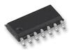
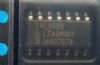
74LVC1G384GW: PinoutDescriptionThe 74LVC1G384GW is one member of the 74LVC1G384 family which is designed as the high-speed Si-gate CMOS device that provides an analog switch, and this switch has input and output ...
SeekIC Buyer Protection PLUS - newly updated for 2013!
268 Transactions
All payment methods are secure and covered by SeekIC Buyer Protection PLUS.
The 74LVC1G384GW is one member of the 74LVC1G384 family which is designed as the high-speed Si-gate CMOS device that provides an analog switch, and this switch has input and output terminals (pins Y and Z) and an active LOW enable input (pin E).
Features of the 74LVC1G384GW are:(1)Very low ON-resistance: 7.5 W (typ) at Vcc = 2.7 V, 6.5 (typ) at Vcc = 3.3 V and 6.0 (typ) at Vcc = 5 V; (2)ESD protection: HBM EIA/JESD22-A114-A exceeds 2 000 V and MM EIA/JESD22-A115-A exceeds 200 V; (3)high noise immunity; (4)CMOS low power consumption; (5)direct interface TTL-levels; (6)latch-up performance meets requirements of JESD78 Class I; (7)multiple package options; (8)specified from -40 °C to +80 °C and -40 °C to +125 °C.
The absolute maximum ratings of the 74LVC1G384GW can be summarized as:(1)supply voltage: -0.5 to +6.5 V;(2)input voltage: -0.5 to +6.5 V;(3)input diode current: -50 mA;(4)switch diode current: ±50 mA;(5)DC switch voltage range: -0.5 to Vcc+0.5 V;(6)DC switch source or sink current: ±50 mA;(7)Vcc or GND current: ±100 mA;(8)storage temperature: -65 to +150 °C;(9)power dissipation: 250 mW. If you want to know more information about the 74LVC1G384GW, please download the datasheet in www.seekic.com or www.chinaicmart.com .