Features: ` Wide supply voltage range from 1.65 to 5.5 V
` High noise immunity
` Complies with JEDEC standard:
JESD8-7 (1.65 V to 1.95 V)
JESD8-5 (2.3 V to 2.7 V)
JESD8B/JESD36 (2.7 V to 3.6 V)
` ±24 mA output drive (VCC = 3.0 V)
` CMOS low power consumption
` Latch-up performance exceeds 250 mA
` Direct interface with TTL levels
` Inputs accept voltages up to 5 V
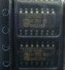
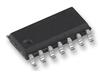
` Multiple package options
` ESD protection:
HBM EIA/JESD22-A114-B exceeds 2000 V
MM EIA/JESD22-A115-A exceeds 200 V.
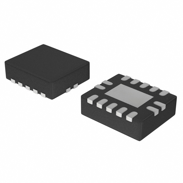
` Specified from -40 °C to +85 °C and -40 °C to +125 °C.Pinout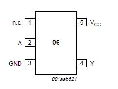
 Specifications
| SYMBOL |
PARAMETER |
CONDITIONS |
MIN. |
MAX. |
UNIT |
| VCC |
supply voltage |
|
-0.5 |
+6.5 |
V |
| IIK |
input diode current |
VI < 0 V |
- |
-50 |
mA |
| VI |
input voltage |
note 1 |
-0.5 |
+6.5 |
V |
| IOK |
output diode current |
VO > VCCor VO < 0 V |
- |
±50 |
mA |
| VO |
output voltage |
active mode; notes 1 and 2 |
-0.5 |
+6.5 |
V |
| Power-down mode; notes 1 and 2 |
-0.5 |
+6.5 |
V |
| IO |
output sink current |
VO = 0 V to VCC |
- |
±50 |
mA |
| ICC, IGND |
VCC or GND current |
|
- |
±100 |
mA |
| Tstg |
storage temperature |
|
-65 |
+150 |
°C |
| Ptot |
power dissipation |
Tamb = -40 °C to +125 °C |
- |
250 |
mW |
Notes
1. The input and output voltage ratings may be exceeded if the input and output current ratings are observed.
2. When VCC = 0 V (Power-down mode), the output voltage can be 5.5 V in normal operation.DescriptionThe 74LVC1G06 is a high-performance, low-power, low-voltage, Si-gate CMOS device, superior to most advanced CMOS compatible TTL families.
Input can be driven from either 3.3 V or 5 V devices. These features allow the use of these devices in a mixed 3.3 V and 5 V environment.
Schmitt trigger action at all inputs makes the circuit tolerant for slower input rise and fall time.
The 74LVC1G06 is fully specified for partial power-down applications using I
off. The I
off circuitry disables the output, preventing the damaging backflow current through the device when it is powered down.
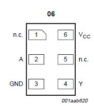
The 74LVC1G06 provides the inverting buffer.
The output of the 74LVC1G06 is an open drain and can be connected to other open-drain outputs to implement active-LOW wired-OR or active-HIGH wired-AND functions.

 74LVC1G06 Data Sheet