Logic Family
:
Number of Bits
:
Counting Method
:
Counting Sequence
:
Operating Supply Voltage
:
Operating Temperature Range
:
Counter Type
: Binary Counters
Packaging
: Tube
Package / Case
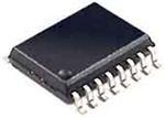
: SOT-109
DescriptionThis action of the 74LVC163D occurs regardless of the levels at CP, PE, CET and CEP inputs This synchronous reset feature enables the designer to modify the maximum count with only one external NAND gate. The look-ahead carry simplifies serial cascading of the counters. Both count enable inputs (CEP and CET) must be HIGH to count. The CET input is fed forward to enable the terminal count output (TC). The TC output thus enabled will produce a HIGH output pulse of a duration approximately equal to a HIGH level output of Q0. This pulse of the 74LVC163D can be used to enable the next cascaded stage. The 74LVC163 is a synchronous presettable binary counter which features an internal look-head carry and can be used for high-speed counting. Synchronous operation is provided by having all flip-flops clocked simultaneously on the positive-going edge of the clock (CP). The outputs (Q0 to Q3) of the counters may be preset to a HIGH or LOW level. A LOW level at the parallel enable input (PE) disables the counting action and causes the data at the data inputs (D0 to D3) to be loaded into the counter on the positive±going edge of the clock (provided that the set-up and hold time requirements for PE are met). Preset takes place regardless of the levels at count enable inputs (CEP and CET). A low level at the master reset input (MR) sets all four outputs of the flip-flops (Q0 to Q3) to LOW level after the next positive-going transition on the clock (CP) input (provided that the set-up and hold time requirements for PE are met). The 74LVC163 is a high-performance, low-power, low-voltage, Si-gate CMOS device and superior to most advanced CMOS compatible TTL families.
The features of 74LVC163D can be summarized as (1)wide supply voltage range of 1.2 V to 3.6 V; (2)in accordance with JEDEC standard no. 8-1A; (3)inputs accept voltages up to 5.5V; (4)CMOS low power consumption; (5)direct interface with TTL levels; (6)synchronous reset; (7)synchronous counting and loading; (8)two count enable inputs for n-bit cascading; (9)positive edge-triggered clock.
The absolute maximum ratings of 74LVC163D are (1)VCC DC supply voltage; (2)-0.5 to +6.5V; (3)IIK DC input diode current V<0: -50mA; (4)VI DC input voltage Note 2: -0.5 to +5.5 V; (5)IOK DC output diode current VO>VCC or VO < 0: ±50mA; (6)VO DC output voltage Note 2: -0.5 to VCC +0.5 V; (7)IO DC output source or sink current VO = 0 to VCC: ±50mA; (8)IGND, ICC DC VCC or GND current: ±100mA; (9)Tstg storage temperature range: -65 to +150°C.(1. Stresses beyond those listed may cause permanent damage to the 74LVC163D. These are stress ratings only and functional operation of the device at these or any other conditions beyond those indicated under arecommended operating conditionso is not implied. Exposure to absolute-maximum-rated conditions for extended periods may affect device reliability. 2. The input and output voltage ratings may be exceeded if the input and output current ratings are observed.)

 74LVC163D Data Sheet


