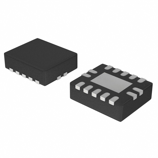
Features: ·5 V tolerant inputs/outputs for interfacing with 5 V logic
·Wide supply voltage range from 1.2 to 3.6 V
·CMOS low power consumption
·MULTIBYTE flow-through standard pin-out architecture
·Low inductance multiple power and ground pins for minimum noise and ground bounce
·Direct interface with TTL levels All data inputs have bushold (74LVCH162373A only)
·High-impedance when VCC = 0 V
·Complies with JEDEC standard no. 8-1A
·ESD protection: HBM EIA/JESD22-A114-A exceeds 2000 V MM EIA/JESD22-A115-A exceeds 200 V.
·Specified from -40 to +85 °C and -40 to +125 °C.
DescriptionThe 74LVC162373A is a 16-bit D-type transparent
latch featuring separate D-type inputs for each latch and 3-state outputs for bus oriented applications. One latch enable (pin nLE) input and one output enable (pin nOE) are provided for each octal. Inputs can be driven from either 3.3 or 5 V devices. In 3-state operation, outputs can handle 5 V. These features allow the use of these devices in a mixed 3.3 and 5 V environment.
The 74LVC162373A consists of 2 sections of eight D-type transparent latches with 3-state true outputs. When pin nLE is HIGH, data at the corresponding data inputs (pins nDn) enter the latches. In this condition the latches are transparent, i.e., a latch output will change each time its corresponding data inputs changes.
When pin nLE is LOW the latches store the information that was present at the data inputs a set-up time preceding the HIGH-to-LOW transition of pin nLE. When pin nOE is LOW, the contents of the eight latches are available at the outputs. When pin nOE is HIGH, the outputs go to the high-impedance OFF-state. Operation of the nOEinput does not affect the state of the latches.
The 74LVC162373A bushold data inputs eliminates the need for external pull-up resistors to hold unused inputs.
The 74LVC162373A is designed with 30series termination resistors in both high and low output stages to reduce line noise.

 74LVC162373A Data Sheet


