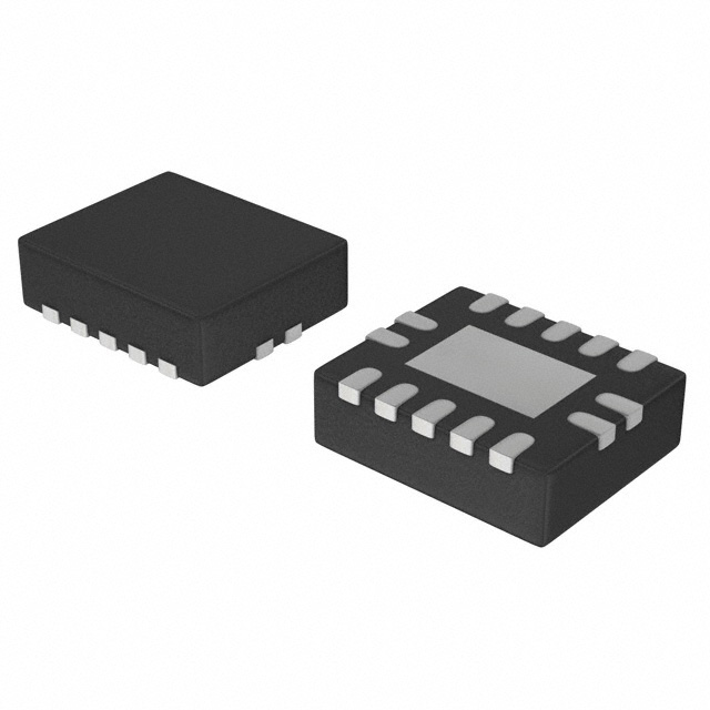
PinoutDescriptionThe 74LVC157APW is designed as one kind of high-performance, low-power, low-voltage, Si-gate CMOS device that is fully specified for partial power-down applications using Ioff. And this device provides one non-inverting buffer/line driver with 3-state output. Features of the 74LV...
74LVC157APW: PinoutDescriptionThe 74LVC157APW is designed as one kind of high-performance, low-power, low-voltage, Si-gate CMOS device that is fully specified for partial power-down applications using Ioff. And ...
SeekIC Buyer Protection PLUS - newly updated for 2013!
268 Transactions
All payment methods are secure and covered by SeekIC Buyer Protection PLUS.
The 74LVC157APW is designed as one kind of high-performance, low-power, low-voltage, Si-gate CMOS device that is fully specified for partial power-down applications using Ioff. And this device provides one non-inverting buffer/line driver with 3-state output.
Features of the 74LVC157APW are:(1)Wide supply voltage range of 1.2 to 3.6 V; (2)In accordance with JEDEC standard no. 8-1A; (3)CMOS lower power consumption; (4)Direct interface with TTL levels; (5)5 Volt tolerant inputs, for interfacing with 5 Volt logic. Also this device is the logic implementation of a 4-pole, 2-position switch, where the position of the switch is determined by the logic levels applied to S.
The absolute maximum ratings of the 74LVC157APW can be summarized as:(1)DC supply voltage:0.5 to +6.5 V;(2)DC input diode current:50 mA;(3)DC input voltage:0.5 to +5.5 V;(4)DC output diode current: +/-50 mA;(5)DC output voltage:0.5 to VCC +0.5 V;(6)DC output diode current: +/-50 mA;(7)DC VCC or GND current: +/-100 mA;(8)Storage temperature range:65 to +150 °C;(9)Power dissipation per package plastic mini-pack (SO): 500 mW;(10)Power dissipation per package plastic shrink mini-pack (SSOP and TSSOP): 500 mW. If you want to know more information about the 74LVC157APW, please download the datasheet in www.seekic.com or www.chinaicmart.com .