Number of Bits
:
Maximum Operating Temperature
: + 125 C
Mounting Style
: SMD/SMT
Supply Voltage - Max
: 3.6 V
Logic Family
: LVC
Packaging
: Tube
Product
: Decoders, Encoders, Multiplexers & Demultiplexers
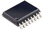
Package / Case
: SOT-109
Number of Lines (Input / Output)
: 8 / 4
Supply Voltage - Min
: 1.2 V
Propagation Delay Time
: 16 ns at 1.2 V, 3 ns at 2.7 V, 2.6 ns at 3.3 V
DescriptionThe 74LVC157AD is designed as a high performance low power, low vltage, sigate CMOS device and superior to most advanced CMOS compatible TTL families. Inputs can be driven from either 3.3 or 5V devices. This feature allows the use of these devices as translators in a mixed 3.3 and 5V environment.
The eight features of the 74LVC157AD. (1)5V tolerant inputs for interfacing with 5V logic. (2)Wide supply voltage range from 1.2 to 3.6V. (3)CMOS low power consumption. (4)Direct interface with TTL levels. (5)Inputs accept voltages up to 5.5V. (6)Complies with JEDEC standard no.8-1A. (7)ESD protection: HBM EIA/JESD22-A114-A exceeds 2000V, MM EIA/JESD22-A115-A exceeds 200V. (8)Specified from -40 to +85°C and -40 to +125°C. Those are all the main features.
Some absolute maximum ratings of the 74LVC157AD have been concluded into several points as follow. (1)Its supply voltage would be min -0.5V and max 6.5V. (2)Its input diode current would be -50mA. (3)Its input voltage would be from -0.5V to 6.5V. (4)Its output diode current would be +/-50mA. (5)Its output voltage would be from -0.5V to Vcc+0.5V. (6)Its output source or sink current would be +/-50mA. (7)Its Vcc or GND current would be +/-100mA. (8)Its storage temperature range would be from -65°C to 150°C. (9)Its power dissipation would be max 500mW. It should be noted that stresses above those listed in absolute maximum ratings may cause permanent damage to device.
Also some electrical characteristics of the 74LVC157AD are concluded as follow. (1)Its high level input voltage would be min Vcc at Vcc=1.2V and would be min 2.0V at Vcc=2.7V to 3.6V. (2)Its low level input voltage would be max GND at Vcc=1.2V and would be max 0.8V at Vcc=2.7V to 3.6V. (3)Its input leakage current of the 74LVC157AD would be typ +/-0.1uA and max +/-5uA. And so on. If you have any question or suggestion or want to know more information please contact us for details. Thank you!

 74LVC157AD Data Sheet


