74LVC125AM

DescriptionThe 74LVC125AM is designed as a low voltage CMOS quad bus buffer fabricated with sub-micron silicon gate and double-layer metal wiring C2MOS technology. It is ideal for 1.65 to 3.6 Vcc operations and low power and low noise applications.The ten features of the 74LVC125AM. (1)5V tolerant...

product image

74LVC125AM Picture
SeekIC No. : 004251207 Detail

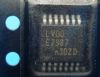
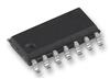
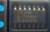
74LVC125AM: DescriptionThe 74LVC125AM is designed as a low voltage CMOS quad bus buffer fabricated with sub-micron silicon gate and double-layer metal wiring C2MOS technology. It is ideal for 1.65 to 3.6 Vcc op...

floor Price/Ceiling Price

Part Number:
74LVC125AM
Supply Ability:
5000

Price Break

  • Qty
  • 1~5000
  • Unit Price
  • Negotiable
  • Processing time
  • 15 Days
Total Cost: $ 0.00

SeekIC Buyer Protection PLUS - newly updated for 2013!

  • Escrow Protection.
  • Guaranteed refunds.
  • Secure payments.
  • Learn more >>

Month Sales

268 Transactions

Rating

evaluate  (4.8 stars)

Upload time: 2024/5/31

Payment Methods

All payment methods are secure and covered by SeekIC Buyer Protection PLUS.

Notice: When you place an order, your payment is made to SeekIC and not to your seller. SeekIC only pays the seller after confirming you have received your order. We will also never share your payment details with your seller.
Product Details

Description


Description

The 74LVC125AM is designed as a low voltage CMOS quad bus buffer fabricated with sub-micron silicon gate and double-layer metal wiring C2MOS technology. It is ideal for 1.65 to 3.6 Vcc operations and low power and low noise applications.

The ten features of the 74LVC125AM. (1)5V tolerant inputs. (2)High speed tPD=4.8ns max at Vcc=3V. (3)Power down protection on inputs and outputs. (4)Symmetrical output impedance: Ioh=Iol=24mA min at Vcc=3V. (5)PCI bus levels guaranteed at 24mA. (6)Balanced propagation delays. (7)Operating voltage range which would be from 1.65V to 3.6V (1.2V data retention). (8)Pin and function compatible with 74 series 125. (9)Latch-up performance exceeds 500mA (JESD 17). (10)ESD performance HBM>2000V (MIL STD 883 method 3015); MM>200V. Those are all the main features.

Some absolute maximum ratings of the 74LVC125AM have been concluded into several points as follow. (1)Its supply voltage would be from -0.5V to 7.0V. (2)Its DC input voltage would be from -0.5V to 7.0V. (3)Its DC output voltage high impedance or Vcc=0V would be from -0.5V to 7V. (4)Its DC output voltage high or low state would be from -0.5V to Vcc+0.5V. (5)Its DC input diode current would be -50mA. (6)Its DC output diode current would be -50mA. (7)Its DC output current would be +/-50mA. (8)Its DC Vcc or ground current per supply pin would be +/-100mA. (9)Its storage temperature range would be from -65°C to 150°C. (10)Its lead temperature 10 seconds would be 300°C. It should be noted that stresses above those listed in absolute maximum ratings may cause permanent damage to device.

Also some electrical characteristics of the 74LVC125AM are concluded as follow. (1)Its high level input voltage would be min 0.65Vcc at Vcc=1.65V to 1.95V and would be min 1.7V at Vcc=2.3V to 2.7V and would be min 2V at Vcc=2.7V to 3.6V. (2)Its low level input voltage would be max 0.35Vcc at Vcc=1.65V to 1.95V and would be max 0.7V at Vcc=2.3V to 2.7V and would be max 0.8V at Vcc=2.7V to 3.6V. And so on. If you have any question or suggestion or want to know more information about the 74LVC125AM please contact us for details. Thank you!


Customers Who Bought This Item Also Bought

Margin,quality,low-cost products with low minimum orders. Secure your online payments with SeekIC Buyer Protection.
Discrete Semiconductor Products
Undefined Category
Cables, Wires
Static Control, ESD, Clean Room Products
Batteries, Chargers, Holders
View more