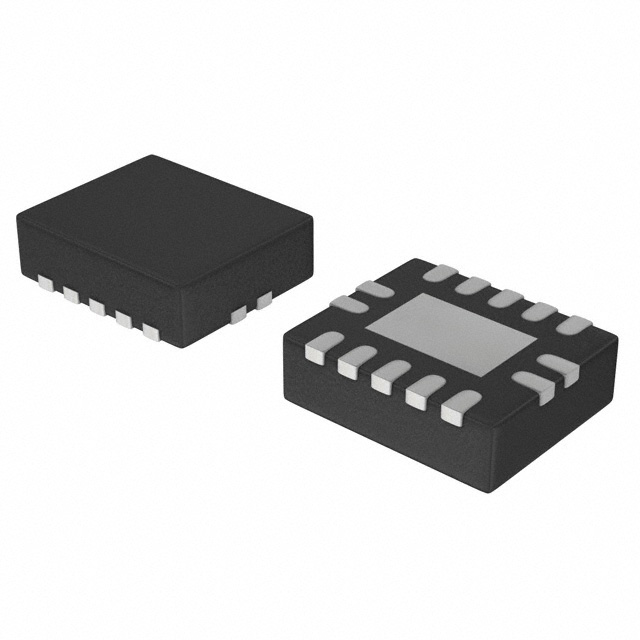
Buffers & Line Drivers 3.3V QUAD 3-S BUS DRIVER
74LVC125AD: Buffers & Line Drivers 3.3V QUAD 3-S BUS DRIVER
SeekIC Buyer Protection PLUS - newly updated for 2013!
268 Transactions
All payment methods are secure and covered by SeekIC Buyer Protection PLUS.
Number of Input Lines : | 4 | Number of Output Lines : | 4 |
Polarity : | Non-Inverting | Supply Voltage - Max : | 3.6 V |
Supply Voltage - Min : | 1.2 V | Maximum Operating Temperature : | + 125 C |
Mounting Style : | SMD/SMT | Package / Case : | SOT-108-14 |
Packaging : | Tube |
The 74LVC125AD is designed as a high performance, low power, low voltage sigate CMOS device and superior to most advanced CMOS compatible TTL families. Inputs can be driven from either 3.3V or 5.0V devices. In 3-state operation, outputs can handle 5V.
The six features of the 74LVC125AD. (1)5V tolerant inputs/outputs, for interfacing with 5V logic. (2)Supply voltage range of 1.2V to 3.6V. (3)Complies with JEDEC standard np.8-1A. (4)CMOS low power consumption. (5)Direct interface with TTL levels. (6)High impedance when Vcc=0V. Those are all the main features.
Some absolute maximum ratings of the 74LVC125AD have been concluded into several points as follow. (1)Its DC supply voltage would be from -0.5V to 6.5V. (2)Its DC input voltage would be from -0.5V to 6.5V. (3)Its DC output voltage output 3-state would be from -0.5V to 6.5V. (4)Its DC output voltage high or low state would be from -0.5V to Vcc+0.5V. (5)Its DC input diode current would be -50mA. (6)Its DC output diode current would be -50mA. (7)Its DC output source or sink current would be +/-50mA. (8)Its DC Vcc or ground current per supply pin would be +/-100mA. (9)Its storage temperature range of the 74LVC125AD would be from -65°C to 150°C. (10)Its power dissipation would be 500mW. It should be noted that stresses above those listed in absolute maximum ratings may cause permanent damage to device.
Also some electrical characteristics of the 74LVC125AD are concluded as follow. (1)Its high level input voltage would be min Vcc at Vcc=1.2V and would be min 2.0V at Vcc=2.7V to 3.6V. (2)Its low level input voltage would be max GND at Vcc=1.2V and would be max 0.8V at Vcc=2.7V to 3.6V. (3)Its high level output voltage would be min Vcc-0.5V at Vcc=2.7V and Io=-12mA. (4)Its low level output voltage would be max 0.4V at Vcc=2.7V and Io=12mA. And so on. If you have any question or suggestion or want to know more information about the 74LVC125AD please contact us for details. Thank you!