Operating Temperature Range
:
Maximum Operating Temperature
: + 125 C
Minimum Operating Temperature
: - 40 C
Number of Circuits
: 6
Logic Type
: CMOS
Logic Family
: 74LVC
High Level Output Current
: - 24 mA
Low Level Output Current
: 24 mA
Packaging
: Tube
Supply Voltage - Max
: 3.6 V
Package / Case
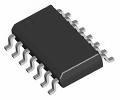
: SOT-108
Supply Voltage - Min
: 1.2 V
Propagation Delay Time
: 14 ns
DescriptionThe 74LVC04AD is designed as one kind of high-performance, low-power, low-voltage, Si-gate CMOS device and superior to most advanced CMOS compat-ible TTL families.
The features of 74LVC04AD are as follows: :(1)5-volt tolerant inputs, for interfacing with 5-volt logic;(2)direct interface with TTL levels;(3)CMOS low power consumption;(4)inputs accept voltages up to 5.5V;(5)complies with JEDEC standard no. 8-1A;(6)wide supply range of 1.2V to 3.6V.
The absolute maximum ratings of the 74LVC04AD are: :(1)DC supply voltage:-0.5 to +6.5 V;(2)DC input diode current:-50 mA;(3)DC input voltage:-0.5 to +5.5 V;(4)DC output diode current:+/-50 mA;(5)DC output voltage:Vcc+0.5 V;(6)DC output source or sink current:+/-50 mA;(7)DC Vcc or GND current:+/-100 mA;(8)storage temperature range:-65 to +150 °C;(9)power dissipation per package--plastic mini-pack (SO):500 mW;(10)power dissipation per package--plastic shrink mini-pack (SSOP and TSSOP):500 mW. Stresses beyond those listed may cause permanent damage to the device. These are stress ratings only and functional operation of the 74LVC04AD at these or any other conditions beyond those indicated under "recommended operating cond-itions" is not implied. Exposure to absolute-maximum-rated conditions for extended periods may affect device reliability.

 74LVC04AD Data Sheet


