Number of Internal Timers
:
Supply Voltage - Max
:
Supply Voltage - Min
:
Maximum Power Dissipation
:
Maximum Operating Temperature
:
Minimum Operating Temperature
:
Type
:
Packaging
: Tube
Package / Case
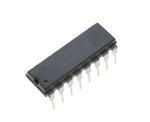
: SOT-38
DescriptionThe 74LV4799N belongs to 74LV4799 family which is a low-voltage Si-gate CMOS control IC for battery management. It consists of: (1)17-stage divider; (2)10-stage up/down counter; (3)control logic; (4)integrated precision oscillator (using external timing components); (5)automatic power-ON reset; (6)scan test facilities; (7)battery charging/full indication output (LED); (8)battery-low indication output (MOLLI); (9)open-drain-N outputs for driving the load transistor. Battery management with the 74LV4799 is based on the principle of time measurement. It measures the charge time, discharge time and self-discharge time by means of a very accurate on-chip oscillator, a divider and an up/down counter.
The features of 74LV4799N can be summarized as (1)wide supply voltage range of 0.9 V to 6 V allows 1 to 4-cell applications; (2)10 V allowed on special inputs; (3)supports virtually all battery chargers, including switched-mode; (4)power supplies; (5)on-chip timer calculates the actual capacity of the battery by; (6)measuring the charger time, discharge time and self-discharge time; (7)automatic switch-over to trickle charge after completion of the; (8)charge time; (9)can be adjusted for use with different types of batteries:-charge time: 4 to 16 hours-discharge time: 15 minutes to 4.7 hours-self-discharge time: 50 to 100 days; (10)battery status indication included:-LED output for charging/full indication- MOLLI output for battery-low indication; (11)LED mode select allows two different methods of indication; (12)automatic power-ON reset; (13)Low-power consumption; (14)requires only a few peripheral components; (15)very accurate on-chip oscillator; (16)scan test facilities included; (17)ICC category of the 74LV4799N: non-standard.
The absolute maximum ratings of 74LV4799N are (1)VCC DC supply voltage(Single sided input protection applied on pins 4, 5, and 9): 0.9(MIN)/1.2(TYP)/6(MAX)V; (2)VI input voltage pins 4, 5, and 9/input voltage pins 7, 13, 14, and 15: 0 to 10/ 0 to VCC V; (3)VO Output voltage pins 10, 11, and 12/Output voltage pins 1, 2, 3, and 6: 0 to VCC/ 0 to 10 V; (4)Tamb operating ambient temperature range in free air (See DC and AC characteristics per device): 0 to +70 °C; (5)input rise and fall times pin 5: 10 ms; (6)tr, tf Input rise and fall times pins 7, 14 and 15: VCC = 1.0V; VI = 1.0V/VCC = 2.0V; VI = 2.0V/VCC = 3.0V; VI = 4.5V/VCC = 3.6V; VI = 6.0V: 500/200/100/50ns; (7)input rise and fall times pin 9: 2s.

 74LV4799N Data Sheet


