Features: • Wide supply voltage range of 0.9 V to 6 V allows 1 to 4-cell applications• 10 V allowed on special inputs• Supports virtually all battery chargers, including switched-mode power supplies• On-chip timer calculates the actual capacity of the battery by measuring t...
74LV4799: Features: • Wide supply voltage range of 0.9 V to 6 V allows 1 to 4-cell applications• 10 V allowed on special inputs• Supports virtually all battery chargers, including switched-m...
SeekIC Buyer Protection PLUS - newly updated for 2013!
268 Transactions
All payment methods are secure and covered by SeekIC Buyer Protection PLUS.
SYMBOL | PARAMETER |
CONDITIONS |
MIN |
MAX |
Unit |
VCC | DC supply voltage |
-0.5 |
+7.0 |
V | |
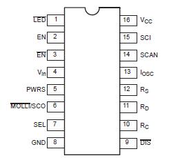
IIK | DC input diode current pins 4, 5 and 9 |
VI < 0.5 or VI > 12 V |
+20 |
mA | |
DC input diode current pins 7, 13, 14 and 15 |
VI < 0.5 or VI > VCC + 0.5 V |
+20 | |||
NON repetitive peak DC input diode current pin 9 |
VI > 10 V and t < 10 s; see note 1 |
10 | |||
VI | DC input voltage range pins 4, 5 and 9 |
-0.5 |
+12 |
V | |
DC input voltage range pins 7, 13, 14 and 15 |
-0.5 |
VCC + 0.5 |
V | ||
IOK | DC output diode current pins 1, 2, 3 and 6 |
VO < 0.5 V |
-20 |
mA | |
IO | DC output sink current pins 1, 2, 3 and 6 |
VO > 0 V |
-25 |
mA | |
IOK | DC output diode current pins 10, 11 and 12 |
VO < 0.5 or VO > VCC + 0.5 V |
±20 |
mA | |
IO | DC output sink or source current pins 10, 11 and 12 |
0.5 V < VO < VCC + 0.5 V |
±25 |
mA | |
IGND, ICC | DC GND or VCC current |
±50 |
mA | ||
Tstg | storage temperature range |
-65 |
+150 |
||
PTOT | Power dissipation per package plastic DIL plastic mini-pack (SO) plastic shrink mini-pack (SSOP and TSSOP) |
for temperature range: 40 to +125°C above +70°C derate linearly with 12 mW/K above +70°C derate linearly with 8 mW/K above +60°C derate linearly with 5.5 mW/K |
750 500 400 |
mW |
NOTES:
1. In applications where a motor is present, the input voltage may exceed the maximum VI, level of 10 V at the DIS nput for a very short period when the motor is switched off.
2. Stresses beyond those listed may cause permanent damage to the device. These are stress ratings only and unctional operation of the device at these or any other conditions beyond those under "recommended operating conditions" is not implied. Exposure to absolute maximum rated conditions for extended periods may affect device eliability.
3. The input and output voltage ratings may be exceeded if the input and output current ratings are observed.
The 74LV4799 is a low-voltage Si-gate CMOS control IC for battery management. The 74LV4799 consists of:
• 17-stage divider
• 10-stage up/down counter
• Control logic
• Integrated precision oscillator (using external timing components)
• Automatic power-ON reset
• Scan test facilities
• Battery charging/full indication output (LED)
• Battery-low indication output (MOLLI)
• Open-drain-N outputs for driving the load transistor
Battery management with the 74LV4799 is based on the principle of time measurement. It measures the charge time, discharge time and self-discharge time by means of a very accurate on-chip oscillator, a divider and an up/down counter.