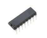
Output Type
:
Minimum Operating Temperature
: - 40 C
Number of Circuits
: 1
Maximum Operating Temperature
: + 125 C
Logic Type
: CMOS
Packaging
: Tube
Counting Sequence
: Up
Number of Input Lines
: 1
Package / Case
: PDIP-16
Counter Type
: Binary Counters
Logic Family
: LV
Propagation Delay Time
: 180 ns
DescriptionThe 74LV4060N belongs to 74LV4060 family which is a low-voltage Si-gate CMOS device and is pin and function compatible with the 74HC/HCT4060. And the 74LV4060 is a 14-stage ripple-carry counter/divider and oscillator with three oscillator terminals (RS, RTC and CTC), ten buffered outputs (Q3 to Q9 and Q11 to Q13) and an overriding asynchronous master reset (MR). The oscillator configuration allows design of either RC or crystal oscillator circuits. The oscillator may be replaced by an external clock signal at input RS. In this case, keep the oscillator pins (RTC and CTC) floating. The counter of the 74LV4060N advances on the negative-going transition of RS. A HIGH level on MR resets the counter (Q3 to Q9 and Q11 to Q13 = LOW), independent of the other input conditions.
The features of 74LV4060N can be summarized as (1)wide operating voltage: 1.0 to 5.5 V; (2)optimized for Low Voltage applications: 1.0 to 3.6 V; (3)accepts TTL input levels between VCC = 2.7 V and VCC = 3.6 V; (4)typical VOLP (output ground bounce) < 0.8 V at VCC = 3.3 V, Tamb = 25°C. typical VOHV (output VOH undershoot) > 2 V at VCC = 3.3 V, Tamb = 25°C.; (5)all active components on chip; (6)RC or crystal oscillator configuration; (7)output capability: standard (except for RTC and CTC); (8)ICC category: MSI.
The absolute maximum ratings of 74LV4060N are (1)VCC DC supply voltage: -0.5 to +7.0V; (2)±IIK DC input diode current(VI < -0.5 or VI > VCC + 0.5V): 20 mA; (3)±IOK DC output diode current(VO < -0.5 or VO > VCC + 0.5V): 50 mA; (4)±IO DC output source or sink current- standard outputs(-0.5V < VO < VCC + 0.5V): 25 mA; (5)±IGND, ±ICC DC VCC or GND current for types with-standard outputs: 50 mA; (6)Tstg storage temperature range of the 74LV4060N: -65 to +150 °C; (7)Ptot power dissipation per package for temperature range: -40 to +125°C,plastic DIL above +70°C derate linearly with 12mW/K/plastic mini-pack (SO) above +70°C derate linearly with 8 mW/K/plastic shrink mini-pack (SSOP and TSSOP)above +60°C derate linearly with 5.5 mW/K: 750/500/400mW.(1. Stresses beyond those listed may cause permanent damage to the device. These are stress ratings only and functional operation of the 74LV4060N at these or any other conditions beyond those indicated under "recommended operating conditions" is not implied. Exposure to absolute maximum rated conditions for extended periods may affect device reliability. 2. The input and output voltage ratings may be exceeded if the input and output current ratings are observed.).

 74LV4060N Data Sheet


