Supply Current
:
Minimum Operating Temperature
: - 40 C
Maximum Operating Temperature
: + 125 C
Supply Voltage - Max
: 6 V
Number of Channels
: 1 Channel
Packaging
: Tube
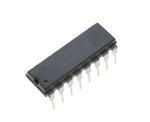
Package / Case
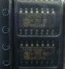
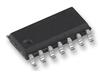
: PDIP-16
Maximum Power Dissipation
: 750 mW
Supply Voltage - Min
: 1 V
On Resistance (Max)
: 145 Ohms
On Time (Max)
: 145 ns
Off Time (Max)
: 145 ns
Propagation Delay Time
: 25 ns, 9 ns, 6 ns, 5 ns, 4 ns, 3 ns
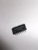
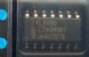
DescriptionThe 74LV4051N belongs to 74LV4051 family which is a low-voltage CMOS device and is pin and function compatible with the 74HC/HCT4051. The 74LV4051 is an 8-channel analog multiplexer/demultiplexer with three digital select inputs (S0 to S2) an active LOW enable input (E), eight independent inputs/outputs (Y0 to Y7) and a common input/output (Z). With E LOW, one of the eight switches is selected (low impedance ON-state) by S0 to S2. With E HIGH, all switches are in the high impedance OFF-state, independent of S0 to S2. VCC and GND of the 74LV4051N are the supply voltage pins for the digital control inputs (S0 to S2, and E). The VCC to GND ranges are 1.0 to 6.0 V. The analog inputs/outputs (Y0 to Y7 and Z) can swing between VCC as a positive limit and VEE as a negative limit. VCC - VEE may not exceed 6.0 V. For operation as a digital multiplexer/demultiplexer, VEE is connected to GND (typically ground).
The features of 74LV4051N can be summarized as (1)optimized for low voltage applications: 1.0 to 6.0 V; (2)accepts TTL input levels between VCC = 2.7 V and VCC = 3.6 V; (3)low typ "ON" resistance: 60 at Vcc ± VEE = 4.5 V, 90 at Vcc ± VEE = 3.0 V, 145 at Vcc ± VEE = 2.0 V; (4)logic level translation: to enable 3V logic to communicate with ±3V analog signals; (5)typical abreak before makeo built in; (6)output capability: non-standard; (7)ICC category: MSI.
The absolute maximum ratings of 74LV4051N are (1)VCC DC supply voltage: -0.5 to +4.6 V; (2)±IIK DC input diode current(VI <-0.5 or VI > VCC + 0.5V): 20mA; (3)±ISK DC switch diode current(VO < -0.5 or VS > VCC + 0.5V): 20mA; (4)±IS DC swith current(-0.5V < VS < VCC + 0.5V): 25mA; (5)Tstg storage temperature range: -65 to +150 °C; (7)power dissipation per package for temperature range: -40 to +125°C-plastic DIL(above +70°C derate linearly with 12mW/K)/-plastic mini-pack (SO)(above +70°C derate linearly with 8 mW/K)/-plastic shrink mini-pack (SSOP and TSSOP)(above +60°C derate linearly with 5.5 mW/K): 750/500/400mW.(1. Stresses beyond those listed may cause permanent damage to the device. These are stress ratings only and functional operation of the 74LV4051N at these or any other conditions beyond those indicated under arecommended operating conditions is not implied. Exposure to absolute-maximum-rated conditions for extended periods may affect device reliability. 2. The input and output voltage ratings may be exceeded if the input and output current ratings are observed.)
 74LV4051N Data Sheet