Features: • Wide operating voltage: 1.0 to 5.5 V
• Optimized for low voltage applications: 1.0 to 3.6 V
• Accepts TTL input levels between VCC = 2.7 V and VCC = 3.6 V
• Typical VOLP (output ground bounce) < 0.8 V at VCC = 3.3 V, Tamb = 25°C
• Typical VOHV (output VOH undershoot) > 2 V at VCC = 3.3 V, Tamb = 25°C
• Output capability: bus driver
• ICC category: MSI
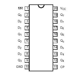
Pinout SpecificationsIn accordance with the Absolute Maximum Rating System (IEC 134)
Voltages are referenced to GND (ground = 0V)
| SYMBOL |
PARAMETER |
CONDITIONS |
RATING |
UNIT |
| VCC |
DC supply voltage |
|
0.5 to +7.0 |
V |
| ±IIK |
DC input diode current |
VI < 0.5 or VI > VCC + 0.5V |
20 |
mA |
| ±IOK |
DC output diode current |
VO < 0.5 or VO > VCC + 0.5V |
50 |
mA |
| ±IO |
DC output source or sink current
standard outputs |
0.5V < VO < VCC + 0.5V |
25 |
mA |
±IGND,
±ICC |
DC VCC or GND current for types with
standard outputs |
|
50
|
mA |
| Tstg |
Storage temperature range |
|
65 to +150 |
°C |
| PTOT |
Power dissipation per package
plastic DIL
plastic mini-pack (SO)
plastic shrink mini-pack (SSOP and TSSOP) |
for temperature range: 40 to +125°C
above +70°C derate linearly with 12mW/K
above +70°C derate linearly with 8 mW/K
above +60°C derate linearly with 5.5 mW/K |
750
500
400 |
mW |
NOTES:
1. Stresses beyond those listed may cause permanent damage to the device. These are stress ratings only and functional operation of the device at these or any other conditions beyond those indicated under "recommended operating conditions" is not implied. Exposure to absolute-maximum-rated conditions for extended periods may affect device reliability.
2. The input and output voltage ratings may be exceeded if the input and output current ratings are observed.
DescriptionThe 74LV273 is a low-voltage Si-gate CMOS device and is pin and function compatible with the 74HC/HCT273.
The 74LV273 has eight edge-triggered , D-type flip-flops with individual D inputs and Q outputs. The common clock (CP) and master reset (MR) inputs load and reset (clear) all flip-flops simultaneously. The state of each D input, one set-up time before the LOW-to-HIGH clock transition, is transferred to the corresponding output (Qn) of the flip-flop.
All outputs of the 74LV273 will be forced LOW independently of clock or data inputs by a LOW voltage level on theMR input.
The device is useful for applications where the true output only is required and the clock and master reset are common to all storage elements.
The 74LV273 is designed as a low-voltage si-gate CMOS device that is pin and function compatible with 74HC/HCT273. It has eight edge-triggered , D-type flip-flops with individual D inputs and Q outputs. The common clock (CP) and master reset inputs load and reset (clear) all flip-flops simultaneously. The state of each D input, one set-up time before the LOW-to-HIGH clock transition, is transferred to the corresponding output (Qn) of the flip-flop.
The features of the 74LV273. The first one is wide operating voltage from 1.0 to 5.5V. The second one is optimized for low voltage applications from 1.0 to 3.6V. The third one is accepts TTL input levels between Vcc=2.7V and Vcc=3.6V. The fourth one is typical Volp (output ground bounce) < 0.8 V at Vcc=3.3V, Tamb = 25°C. The fifth one is typical Vohv (output Voh undershoot) > 2V at Vcc=3.3V, Tamb = 25°C. The sixth one is ideal buffer for MOS microprocessor or memory. The seventh one is common clock and master reset. The eighth one is its output capability is standard. The ninth one is its ICC category is MSI. That are all the main features.
Some absolute maximum ratings of the 74LV273 have been concluded into several points as follow. The first one is about its DC supply voltage which would be from 0.5 to +7.0V. The second one is about its DC input diode current which would be 20mA. The third one is about its DC output diode current which would be 50mA. The fourth one is about its DC output source or sink current standard outputs which would be 25mA. The fifth one is about its DC Vcc or GND current for types with standard outputs which would be 50mA. The sixth one is about its storage temperature range which would be from 65 to +150°C. The seventh one is about its power dissipation per package which would be 750mW for plastic DIL and would be 500mW for plastic mini-pack (SO) and would be 400mW for plastic shrink mini-pack (SSOP and TSSOP). It should be noted that stresses beyond those listed may cause permanent damage to the device. Exposure to absolute maximum rated conditions for extended periods may affect device reliability. And so on. For more information please contact us for details.

 74LV273 Data Sheet


