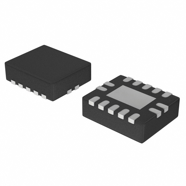
Features: • Wide operating voltage: 1.0 to 5.5 V• Optimized for low voltage applications: 1.0 to 3.6 V• Accepts TTL input levels between VCC = 2.7 V and VCC = 3.6 V• Typical VOLP (output ground bounce) < 0.8 V at VCC = 3.3 V, Tamb = 25°C• Typical VOHV (output VOH u...
74LV165: Features: • Wide operating voltage: 1.0 to 5.5 V• Optimized for low voltage applications: 1.0 to 3.6 V• Accepts TTL input levels between VCC = 2.7 V and VCC = 3.6 V• Typical ...
SeekIC Buyer Protection PLUS - newly updated for 2013!
268 Transactions
All payment methods are secure and covered by SeekIC Buyer Protection PLUS.
SYMBOL | PARAMETER | CONDITIONS | RATING | UNIT |
VCC | DC supply voltage | 0.5 to +7.0 | V | |
±IIK | DC input diode current | VI < 0.5 or VI > VCC + 0.5V | 20 | mA |
±IOK | DC output diode current | VO < 0.5 or VO > VCC + 0.5V | 50 | mA |
±IO | DC output source or sink current standard outputs |
0.5V < VO < VCC + 0.5V | 25 | mA |
±IGND, ±ICC |
DC VCC or GND current for types with standard outputs |
50 |
mA | |
Tstg | Storage temperature range | 65 to +150 | °C | |
PTOT | Power dissipation per package plastic DIL plastic mini-pack (SO) plastic shrink mini-pack (SSOP and TSSOP) |
for temperature range: 40 to +125°C above +70°C derate linearly with 12mW/K above +70°C derate linearly with 8 mW/K above +60°C derate linearly with 5.5 mW/K |
750 500 400 |
mW |
The 74LV165 is designed as a low-voltage si-gate CMOS device that is pin and function compatible with 74HC/HCT165. It is an 8-bit parallel-load or serial-in shift register with complementary serial outputs available from the last stage.
The features of the 74LV165. The first one is wide operating voltage from 1.0 to 5.5V. The second one is optimized for low voltage applications from 1.0 to 3.6V. The third one is accepts TTL input levels between Vcc=2.7V and Vcc=3.6V. The fourth one is typical Volp (output ground bounce) < 0.8 V at Vcc=3.3V, Tamb = 25°C. The fifth one is typical Vohv (output Voh undershoot) > 2V at Vcc=3.3V, Tamb = 25°C. The sixth one is asynchronous 8-bit parallel load. The seventh one is synchronous serial input. The eighth one is its output capability is standard. The ninth one is its ICC category is MSI. That are all the main features.
Some absolute maximum ratings of the 74LV165 have been concluded into several points as follow. The first one is about its DC supply voltage which would be from 0.5 to +7.0V. The second one is about its DC input diode current which would be 20mA. The third one is about its DC output diode current which would be 50mA. The fourth one is about its DC output source or sink current standard outputs which would be 25mA. The fifth one is about its DC Vcc or GND current for types with standard outputs which would be 50mA. The sixth one is about its storage temperature range which would be from 65 to +150°C. The seventh one is about its power dissipation per package which would be 750mW for plastic DIL and would be 500mW for plastic mini-pack (SO) and would be 400mW for plastic shrink mini-pack (SSOP and TSSOP). It should be noted that stresses beyond those listed may cause permanent damage to the 74LV165. Exposure to absolute maximum rated conditions for extended periods may affect device reliability. And so on. For more information please contact us for details.
The 74LV165 is a low-voltage Si-gate CMOS device and is pin and function compatible with 74HC/HCT165.
The 74LV165 is an 8-bit parallel-load or serial-in shift register with complementary serial outputs (Q7 and Q7) available from the last stage. When the arallel load (PL) input is LOW, parallel data from the D0 to D7 inputs are loaded into the register asynchronously. When PL is HIGH, data enters the register serially at the DS input and shifts one place to the right (Q0"Q1"Q2, etc.) with each positive-going clock transition. This feature allows parallel-to-serial converter expansion by tying the Q7 output to the DS input of the succeeding stage.
The clock input is a gated-OR structure which allows one input to be used as an active LOW clock enable (CE) input. The pin assignment for the CP andCE inputs is arbitrary and can be reversed for layout convenience. The LOW-to-HIGH transition of inputCE should only take place while CP HIGH for predictable operation. Either the CP or theCE should be HIGH before the LOW-to-HIGH transition ofPL to prevent shifting the data whenPL is activated.