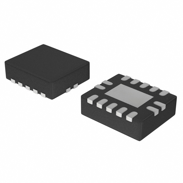
Features: • Wide operating voltage: 1.0 to 5.5 V
• Optimized for low voltage applications: 1.0 to 3.6 V
• Accepts TTL input levels between VCC = 2.7 V and VCC = 3.6 V
• Typical VOLP (output ground bounce) < 0.8 V at VCC = 3.3 V, Tamb = 25°C
• Typical VOHV (output VOH undershoot) > 2 V at VCC = 3.3 V, Tamb = 25°C
• Demultiplexing capability
• Multiple input enable for easy expansion
• Ideal for memory chip select decoding
• Active LOW mutually exclusive outputs
• Output capability: standard
• ICC category: MSIPinout Specifications
In accordance with the Absolute Maximum Rating System (IEC 134)
Voltages are referenced to GND (ground = 0V)
| SYMBOL |
PARAMETER |
CONDITIONS |
RATING |
UNIT |
| VCC |
DC supply voltage |
|
0.5 to +7.0 |
V |
| ±IIK |
DC input diode current |
VI < 0.5 or VI > VCC + 0.5V |
20 |
mA |
| ±IOK |
DC output diode current |
VO < 0.5 or VO > VCC + 0.5V |
50 |
mA |
| ±IO |
DC output source or sink current
standard outputs |
0.5V < VO < VCC + 0.5V |
25 |
mA |
±IGND,
±ICC |
DC VCC or GND current for types with
standard outputs |
|
50
|
mA |
| Tstg |
Storage temperature range |
|
65 to +150 |
°C |
| PTOT |
Power dissipation per package
plastic DIL
plastic mini-pack (SO)
plastic shrink mini-pack (SSOP and TSSOP) |
for temperature range: 40 to +125°C
above +70°C derate linearly with 12 mW/K
above +70°C derate linearly with 8 mW/K
above +60°C derate linearly with 5.5 mW/K |
750
500
400 |
mW |
NOTE:
1. Stresses beyond those listed may cause permanent damage to the device. These are stress ratings only and functional operation of the device at these or any other conditions beyond those indicated under "recommended operating conditions" is not implied. Exposure to absolute-maximum-rated conditions for extended periods may affect device reliability.
2. The input and output voltage ratings may be exceeded if the input and output current ratings are observed.
Description
The 74LV138 is a low-voltage Si-gate CMOS device that is pin and function compatible with 74HC/HCT138.
The 74LV138 accepts three binary weighted address inputs (A0, A1, A2) and when enabled, provide 8 mutually exclusive active LOW outputs (Y0 to Y7).
The 74LV138 features three enable inputs: two active LOW (E1, and E2) and one active HIGH (E3). Every output will be HIGH unless E1 and E2 are LOW and E3 is HIGH.
This multiple enable function allows easy parallel expansion of the 74LV138 to a 1-of-32 (5 lines to 32 lines) decoder with just four 74LV138 ICs and one inverter. The 74LV138 can be used as an eight output demultiplexer by using one of the active LOW enable inputs as the data input and the remaining enable inputs as strobes. Unused enable inputs must be permanently tied to their appropriate active HIGH or LOW state. The 74LV138 is identical to the 74LV238 but has non-inverting (true) outputs.
The 74LV138 is designed as a low-voltage si-gate CMOS device that is pin and function compatible with 74HC/HCT138. It accepts three binary weighted address inputs (A0, A1, A2) and when enabled, provide 8 mutually exclusive active LOW outputs.
The features of the 74LV138. The first one is wide operating voltage from 1.0 to 5.5V. The second one is optimized for low voltage applications from 1.0 to 3.6V. The third one is accepts TTL input levels between Vcc=2.7V and Vcc=3.6V. The fourth one is typical Volp (output ground bounce) < 0.8 V at Vcc=3.3V, Tamb = 25°C. The fifth one is typical Vohv (output Voh undershoot) > 2V at Vcc=3.3V, Tamb = 25°C. The sixth one is demultiplexing capability. The seventh one is multiple input enable for easy expansion. The eighth one is it would be ideal for memory chip select decoding. The ninth one is active low mutually exclusive outputs. The tenth one is its output capability is standard. The eleventh one is its ICC category is MSI. That are all the main features.
Some absolute maximum ratings of the 74LV138 have been concluded into several points as follow. The first one is about its DC supply voltage which would be from 0.5 to +7.0V. The second one is about its DC input diode current which would be 20mA. The third one is about its DC output diode current which would be 50mA. The fourth one is about its DC output source or sink current standard outputs which would be 25mA. The fifth one is about its DC Vcc or GND current for types with standard outputs which would be 50mA. The sixth one is about its storage temperature range which would be from 65 to +150°C. The seventh one is about its power dissipation per package which would be 750mW for plastic DIL and would be 500mW for plastic mini-pack (SO) and would be 400mW for plastic shrink mini-pack (SSOP and TSSOP). It should be noted that stresses beyond those listed may cause permanent damage to the device. And so on. For more information please contact us for details.

 74LV138 Data Sheet


