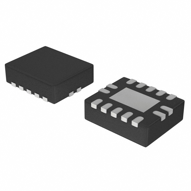
74LV125N

DescriptionThe 74LV125N is a low-voltage Si-gate CMOS device and is pin and function compatible with 74HC/HCT125. The 74LV125 consists of four non-inverting buffers/line drivers with 3-state outputs. The 3-state outputs (nY) are controlled by the output enable input (nOE). A HIGH at nOE causes the...

product image

74LV125N Picture
SeekIC No. : 004251131 Detail

74LV125N: DescriptionThe 74LV125N is a low-voltage Si-gate CMOS device and is pin and function compatible with 74HC/HCT125. The 74LV125 consists of four non-inverting buffers/line drivers with 3-state outputs...

floor Price/Ceiling Price

Part Number:
74LV125N
Supply Ability:
5000

Price Break

  • Qty
  • 1~5000
  • Unit Price
  • Negotiable
  • Processing time
  • 15 Days
Total Cost: $ 0.00

SeekIC Buyer Protection PLUS - newly updated for 2013!

  • Escrow Protection.
  • Guaranteed refunds.
  • Secure payments.
  • Learn more >>

Month Sales

268 Transactions

Rating

evaluate  (4.8 stars)

Upload time: 2024/11/23

Payment Methods

All payment methods are secure and covered by SeekIC Buyer Protection PLUS.

Notice: When you place an order, your payment is made to SeekIC and not to your seller. SeekIC only pays the seller after confirming you have received your order. We will also never share your payment details with your seller.
Product Details

Description


Description

The 74LV125N is a low-voltage Si-gate CMOS device and is pin and function compatible with 74HC/HCT125. The 74LV125 consists of four non-inverting buffers/line drivers with 3-state outputs. The 3-state outputs (nY) are controlled by the output enable input (nOE). A HIGH at nOE causes the outputs to assume a high impedance OFF-state.

The features of 74LV125N can be summarized as (1)wide operating voltage: 1.0 to 5.5 V; (2)optimized for low voltage applications: 1.0 to 3.6 V; (3)accepts TTL input levels between VCC = 2.7 V and VCC = 3.6 V; (4)typical VOLP (output ground bounce) < 0.8 V at VCC = 3.3 V, Tamb = 25°C.; (5)typical VOHV (output VOH undershoot) > 2 V at VCC = 3.3 V, TAMB = 25°C; (6)output capability: standard; (7)ICC category: MSI

The absolute maximum ratings of 74LV125N are (1)VCC DC supply voltage: -0.5(MIN)/+7.0(MAX)V; (2)Tstg storage temperature range: -65 to +150°C; (3)±IIK DC input diode current(VI < -0.5 V; note 1): 20mA(MAX); (4)±IOK DC output diode current( VO <-0.5 V or VO > VCC+ 0.5 V; note 1): 50mA; (5)IO DC output source or sink current(-0.5 V < VO < VCC + 0.5 V): 35mA; (6)±IGND, ±ICC DC VCC or GND current for types with-standard outputs: 70mA; (7)PTOT power dissipation per package(for temperature range: -40 to +125°C) - plastic DIL(above +70°C derate linearly with 12 mW/K) - plastic mini-pack (SO) (SSOP and TSSOP)(above +70°C derate linearly with 8 mW/K)- plastic shrink mini-pack(above +60°C derate linearly with 5.5mW/K): 750/500/400mW.((NOTE: 1. Stresses beyond those listed may cause permanent damage to the device. These are stress ratings only and functional operation of the 74LV125N at these or any other conditions beyond those indicated under arecommended operating conditionso is not implied. Exposure to absolute-maximum-rated conditions for extended periods may affect device reliability. 2. The input and output voltage ratings may be exceeded if the input and output current ratings are observed).


Customers Who Bought This Item Also Bought

Margin,quality,low-cost products with low minimum orders. Secure your online payments with SeekIC Buyer Protection.
Boxes, Enclosures, Racks
RF and RFID
Power Supplies - Board Mount
Circuit Protection
View more