74HC/HCT4046A

Features: Low power consumption Centre frequency of up to 17 MHz (typ.) at VCC=4.5V Choice of three phase comparators: EXCLUSIVE-OR; edge-triggered JK flip-flop; edge-triggered RS flip-flop Excellent VCO frequency linearity VCO-inhibit control for ON/OFF keying and for low stand by power consumpt...

product image

74HC/HCT4046A Picture
SeekIC No. : 004250680 Detail

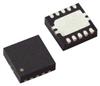
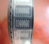
74HC/HCT4046A: Features: Low power consumption Centre frequency of up to 17 MHz (typ.) at VCC=4.5V Choice of three phase comparators: EXCLUSIVE-OR; edge-triggered JK flip-flop; edge-triggered RS flip-flop Excelle...

floor Price/Ceiling Price

Part Number:
74HC/HCT4046A
Supply Ability:
5000

Price Break

  • Qty
  • 1~5000
  • Unit Price
  • Negotiable
  • Processing time
  • 15 Days
Total Cost: $ 0.00

SeekIC Buyer Protection PLUS - newly updated for 2013!

  • Escrow Protection.
  • Guaranteed refunds.
  • Secure payments.
  • Learn more >>

Month Sales

268 Transactions

Rating

evaluate  (4.8 stars)

Upload time: 2024/5/9

Payment Methods

All payment methods are secure and covered by SeekIC Buyer Protection PLUS.

Notice: When you place an order, your payment is made to SeekIC and not to your seller. SeekIC only pays the seller after confirming you have received your order. We will also never share your payment details with your seller.
Product Details

Description


Features:

Low power consumption
Centre frequency of up to 17 MHz (typ.) at VCC=4.5V
Choice of three phase comparators: EXCLUSIVE-OR;
    edge-triggered JK flip-flop;
    edge-triggered RS flip-flop
Excellent VCO frequency linearity
VCO-inhibit control for ON/OFF keying and for low
    stand by power consumption
Minimal frequency drift
Operating power supply voltage range:
    VCO section 3.0 to 6.0V
    digital section 2.0 to 6.0V
Zero voltage offset due to op-amp buffering
Output capability: standard
  ICC category: MSI.


Application

• FM modulation and demodulation
• Frequency synthesis and multiplication
• Frequency discrimination
• Tone decoding
• Data synchronization and conditioning
• Voltage-to-frequency conversion
• Motor-speed control.


Pinout

  Connection Diagram


Specifications

SYMBOL PARAMETER MAX. MIN. UNIT CONDITIONS
VCC DC supply voltage −0.5 +7 V  
±IIK DC input diode current   20 mA For VI<−0.5V or VI>VCC+0.5V
±IOK DC input diode current   20 mA For VO<−0.5V or VO>VCC+0.5V
±IO DC output source or sink current   25 mA For −0.5V<VO<VCC+0.5V
±ICC;±IGND DC VCC or GND current   50 mA  
Tstg storage temperature range −65 +150 °C  
Ptot power dissipation per package plastic DIL   750 mW

for temperature range:
−40to +125°C74HC/HCT
above+70°C:derate linearly with 12 mW/K

plastic mini-pack (SO)   500 mW above+70°C:derate linearly with 8 mW/K


Description

The 74HC/HCT4046A are high-speed Si-gate CMOS devices and are pin compatible with the "4046" of the "4000B" series. They are specified in compliance with JEDEC standard no. 7A.

The 74HC/HCT4046A are phase-locked-loop circuits that comprise a linear voltage-controlled oscillator (VCO) and three different phase comparators (PC1, PC2 and PC3) with a common signal input amplifier and a common comparatorinput.

The signal input of the 74HC/HCT4046A can be directly coupled to large voltage signals, or indirectly coupled (with a series capacitor) to small voltage signals. A self-bias input circuit keeps small voltage signals within the linear region of the input amplifiers. With a passive low-pass filter, the "4046A" forms a second-order loop PLL. The excellent VCO linearity is achieved by the use of linear op-amp techniques.

The VCO requires one external capacitor C1 (betweenCA and C1B)and one external resistor R1 (betweenR1and GND) or two external resistors R1 and R2(between R1and GND, and R2and GND). Resistor R1 and capacitor C1 determine the frequency range of the VCO. Resistor R2 enables the VCO to have a frequency offset if required.

The high input impedance of the VCO simplifies the design of low-pass filters by giving the designer a wide choice of resistor/capacitor ranges. In order not to load the low-pass filter, a demodulator output of the VCO input voltage isprovided at pin10 (DEMOUT). In contrast to conventional techniques where the DEM OUT voltage is one threshold voltage lower than the VCO input voltage, here the DEM OUT voltage equals that of the VCO input. If DEMOUT is used, a load resistor (RS)should be connected from DEMOUT to GND; if unused, DEMOUT  of the 74HC/HCT4046A should be left open. The VCO output (VCOOUT)can be connected directly to the comparator input (COMPIN), or connectedvia a frequency-divider. The VCO output signal has a duty factor of 50% (maximum expected deviation 1%), if the VCO input is held at a constant DC level. A LOW level at the inhibit input (INH)enables the VCO and demodulator, while a HIGH level turns both off to minimize standby power consumption.

The only difference between the HC and HCT versions of the 74HC/HCT4046A is the input level specification of the INH input. This input disables the VCO section. The sections of the comparator are identical, so that there is no difference in the SIGIN(pin14) or COMPIN (pin3) inputs between the HC and HCT versions.


Customers Who Bought This Item Also Bought

Margin,quality,low-cost products with low minimum orders. Secure your online payments with SeekIC Buyer Protection.
Sensors, Transducers
Undefined Category
Resistors
Industrial Controls, Meters
View more