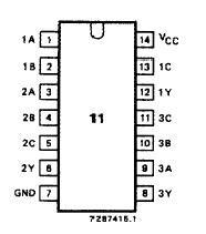
Features: · Output capability: standard· ICC category: SSIPinoutDescriptionThe 74HCT11 is high-speed Si-gate CMOS devices and are pin compatible with low power Schottky TTL (LSTTL). They are specified in compliance with JEDEC standard no. 7A. The 74HC/HCT11 provide the 3-input AND function. The 7...
74HCT11: Features: · Output capability: standard· ICC category: SSIPinoutDescriptionThe 74HCT11 is high-speed Si-gate CMOS devices and are pin compatible with low power Schottky TTL (LSTTL). They are specifi...
SeekIC Buyer Protection PLUS - newly updated for 2013!
268 Transactions
All payment methods are secure and covered by SeekIC Buyer Protection PLUS.
Features: · Output capability: standard· ICC category: SSIPinoutDescription The 74HC/HCT02 are hig...
Features: · Level shift capability· Output capability: standard (open drain)· ICC category: SSIPin...
The 74HCT11 is high-speed Si-gate CMOS devices and are pin compatible with low power Schottky TTL (LSTTL). They are specified in compliance with JEDEC standard no. 7A. The 74HC/HCT11 provide the 3-input AND function.
The 74HCT11 is designed as a high-speed si-gate CMOS device and is pin compatible with low power schottky TTL (LSTTL). It is specified in compliance with JEDEC standard no. 7A. The 74HC11 provide the 3-input AND function. It has two features which means its output capability would be standard and its ICC category would be SSI.
Some important AC characteristics and specifications of the 74HCT11 have been concluded into several points as follow.For Tamb=25°C the first one is about its propagation delay which would be typ 32ns and max 100ns at Vcc=2.0V and would be typ 12ns and max 20ns at Vcc=4.5V and would be typ 10ns and max 17ns at Vcc=6.0V. The second one is about its output transition time which would be typ 19ns and max 75ns at Vcc=2.0V and typ 7ns and max 15ns at Vcc=4.5V and would be typ 6ns and max 13ns at Vcc=6.0V.
Also for the Tamb range of the 74HCT11 -40 to +85°C the first one is about its propagation delay which would be max 125ns at Vcc=2.0V and would be max 25ns at Vcc=4.5V and would be max 21ns at Vcc=6.0V. The second one is about its output transition time which would be max 95ns at Vcc=2.0V and max 19ns at Vcc=4.5V and would be max 16ns at Vcc=6.0V. For the Tamb range of -40 to +125°C the first one is about its propagation delay which would be max 150ns at Vcc=2.0V and would be max 30ns at Vcc=4.5V and would be max 26ns at Vcc=6.0V. The second one is about its output transition time which would be max 110ns at Vcc=2.0V and max 22ns at Vcc=4.5V and would be max 19ns at Vcc=6.0V. And so on. For more information about the 74HCT11 please contact us.
And some pin description about the 74HCT11. Its pin 1, 3, 9 would be for data inputs. Its pin 2, 4, 10 would also be for data inputs. Its pin 7 would be ground (0V). Its pin 12, 6, 8 would be data outputs. Its pin 13, 5, 11 would be for data inputs. Its pin 14 would be Vcc that of positive supply voltage. And so on. For more information please contact us.