Number of Channels
:
Supply Current
:
Maximum Power Dissipation
: 500 mW
Minimum Operating Temperature
: - 40 C
Maximum Operating Temperature
: + 125 C
Supply Voltage - Min
: 2 V
On Resistance (Max)
: 180 Ohms
Packaging
: Tube
Propagation Delay Time
: 60 ns, 12 ns, 10 ns, 8 ns
On Time (Max)
: 220 ns
Off Time (Max)
: 210 ns
Supply Voltage - Max
: 10 V
Package / Case
: SO
Pinout Description
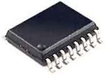
74HC4053D is a high-speed Si-gate CMOS device, which is specified in compliance with JEDEC standard no.7A.The 74HC4053D is triple 2-channel analog multiplexer/demultiplexer with acommon enable input (E). Each multiplexer/ demultiplexer has two independent inputs/outputs (nY0 and nY1), a common input/output (nZ) and three digital select inputs (Sn).one of the two switches is choosed (low-impedance ON-state) by S1 to S3. With E HIGH, all switches are in the high-impedance OFF-state, independent of S1 to S3.VCC and GND are the supply voltage pins for the digital control inputs (S1 to S3 and E).The VCC to GND ranges are from 2.0 V to 10.0 V for 74HC4053D and from 4.5 V to 5.5 V for 74HCT4053D. The analog inputs/outputs (nY0 and nY1, and nZ) can swing between VCC as a positive limit and VEE as a negative limit. VCC - VEE may not exceed 10.0 V. For operation as a digital multiplexer/ demultiplexer, VEE is connected to GND (typically ground).
The unique features of the 74HC4053D is shown as below:(1)low ON resistance when 80 (typical) at VCC - VEE is4.5 V,70 (typical) at VCC - VEE is 6.0 V,and 60 (typical) at VCC - VEE is 9.0 V(2) Logic level translation enables 5 V logic to communicate with ±5 V analog signals;(3)Typical "break before make" built in;(4) Complies with JEDEC standard no. 7A;(5)ESD protection while HBM EIA/JESD22-A114-C exceeds 2000 V and MM EIA/JESD22-A115-A exceeds 200 V;(6)Multiple package options;(7) Specified from -40 to +85 and from -40 to +125 .etc
74HC4053D also has the following quick reference data and limiting values. The reference data:(1): independent I/O (nYn) is 5 pF;(2):common I/O (nZ) is 8 pF;(3):power dissipation capacitance is 36 pF when per switch and VI is GND to VCC.The limiting values(In accordance with the absolute maximum rating system.Voltages are referenced toVEE= GND ):(1):supply voltage is -0.5V min and +11.0 V max;(2):input clamping current is ±20 mA max when VI is greater than -0.5 V or VI is greater than VCC+0.5 V;(3)The switch clamping current of the 74HC4053D is ±20 mA max when VS is greater than-0.5 V or VS is greater than VCC+0.5 V;(4):switch current is ±25 mA max; (5):negative supply current is -20 mA max;(6):quiescent supply current is 50 mA max;(7):ground current is 50 mA max;(8):storage temperature is -65 min and +150 .

 74HC4053D Data Sheet


