Features: ` Low "ON" resistance:
80 (typ.) at VCC - VEE = 4.5 V
70 (typ.) at VCC - VEE = 6.0 V
60 (typ.) at VCC - VEE = 9.0 V
` Logic level translation:
to enable 5 V logic to communicate
with ± 5 V analog signals
` Typical "break before make" built in
` Output capability: non-standard
` ICC category: MSI Application· Analog multiplexing and demultiplexing
· Digital multiplexing and demultiplexing
· Signal gatingPinout Specifications
| SYMBOL |
PARAMETER |
MIN. |
MAX. |
UNIT |
CONDITIONS |
| VCC |
DC supply voltage |
-0.5 |
+11.0 |
V |
|
| ±IIK |
DC digital input diode current |
|
20 |
mA |
for VI < -0.5 V or VI > VCC + 0.5 V |
| ±ISK |
DC switch diode current |
|
20 |
mA |
for VS < -0.5 V or VS > VCC + 0.5 V |
| ±IS |
DC switch current |
|
25 |
mA |
for -0.5 V < VS < VCC + 0.5 V |
| ±IEE |
DC VEE current |
|
20 |
mA |
|
| ±ICC; ±IGND |
DC VCC or GND current |
|
50 |
mA |
|
| Tstg |
storage temperature range |
-65 |
+150 |
°C |
|
| Ptot |
power dissipation per package
plastic DIL |
|
750 |
mW |
for temperature range: -40 to + 125 °C
74HC/HCT
above + 70 °C: derate linearly with 12 mW/K |
| |
plastic mini-pack (SO) |
|
500 |
mW |
above + 70 °C: derate linearly with 8 mW/K |
| PS |
power dissipation per switch |
|
100 |
mW |
|
DescriptionThe 74HC257 is high-speed Si-gate CMOS devices and are pin compatible with the "4053" of the "4000B" series. They are specified in compliance with JEDEC standard no. 7A.
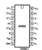
The 74HC257 is triple 2-channel analog multiplexers/demultiplexers with a common enable input (E). Each multiplexer/demultiplexer has two independent inputs/outputs (nY0 and nY1), a common input/output (nZ) and three digital select inputs (S1 to S3).
With E LOW, one of the two switches is selected (low impedance ON-state) by S1 to S3. With E HIGH, all switches are in the high impedance OFF-state, independent of S1 to S3.
VCC and GND of the 74HC257 are the supply voltage pins for the digital control inputs (S1, to S3, and E). The VCC to GND ranges are 2.0 to 10.0 V for HC and 4.5 to 5.5 V for HCT. The analog inputs/outputs (nY0 and nY1, and nZ) can swing between VCC as a positive limit and VEE as a negative limit.VCC - VEE may not exceed 10.0 V.
For operation of the 74HC257 as a digital multiplexer/demultiplexer, VEE is connected to GND (typically ground).

 74HC257 Data Sheet


