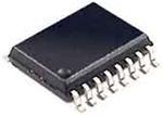
Maximum Operating Temperature
: + 125 C
Mounting Style
: SMD/SMT
Number of Circuits
: 2
Input Type
: Single-Ended
Packaging
: Tube
Polarity
: Inverting/Non-Inverting
Output Type
: Differential
High Level Output Current
: - 7.8 mA
Low Level Output Current
: 7.8 mA
Supply Voltage - Max
: 6 V
Logic Family
: HC
Package / Case
: SOT-109
Logic Type
: J-K Negative Edge Triggered Flip Flop
Propagation Delay Time
: 15 ns at 5 V
DescriptionThe 74HC112D high speed J-K Flip-Flops utilize advanced silicon-gate CMOS technology to achieve the low power consumption and high noise immunity of standard CMOS intergated circuits, along with the ability to drive 10 LS-TTL loads. The feature of 74HC112D are as follows: (1)typical propagation delay: 16ns; (2)wide operating voltage range; (3)low input current: 1A maximum; (4)low quiescent current: 40A; (5)high output drive: 10 LS-TTL loads.
The absolute maximum ratings of the 74HC112D are: (1)supply voltage: -0.5 to +7.0V; (2)DC input voltage: -1.5 to Vcc +1.5V; (3)DC output voltage: -0.5 to Vcc +0.5V; (4)clamp diode current: ±20mA; (5)DC output current, per pin: ±25mA; (6)DC VCC or GND current, per pin: ±50mA; (7)stprage temperature range: -65 to +150; (8)power dissipation: 600mW; (9)lead temp.: 260.
The following is about the electrical characteristics of 74HC112D: (1)minimum high level input voltage: 1.5V; (2)maximum low level input voltage: 0.5V; (3)minimum high level output voltage: 1.9V at VIN=VIH or VIL, IOUT20A or 3.84V at VIN=VIH or VIL, IOUT4.0mA; (4)maximum low level output voltage: 0.1V at VIN=VIH or VIL, IOUT20A or 0.33V at VIN=VIH or VIL, IOUT4.0mA; (5)maximum input current: ±1.0A at VIN=VCC or GND; (6)maximum quiescent supply current: 40A at VIN=VCC or GND, IOUT=0A.

 74HC112D Data Sheet


