Features: FEATURES:•Common features:0.5 MICRON CMOS TechnologyHigh-speed, low-power CMOS replacement forABT functionsTypical tSK(o) (Output Skew) < 250psLow input and output leakage 1µA (max.)ESD > 2000V per MIL-STD-883, Method 3015;> 200V using machine model (C = 200pF, R = 0...
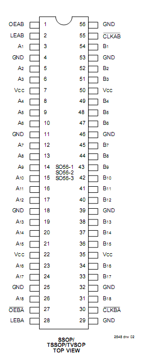
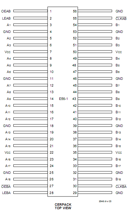
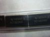
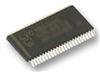
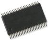
74FCT162500AT: Features: FEATURES:•Common features:0.5 MICRON CMOS TechnologyHigh-speed, low-power CMOS replacement forABT functionsTypical tSK(o) (Output Skew) < 250psLow input and output leakage 1µ...
SeekIC Buyer Protection PLUS - newly updated for 2013!
268 Transactions
All payment methods are secure and covered by SeekIC Buyer Protection PLUS.
Features: Std., A and C speed gradesLow input and output leakage ?1A (max.)CMOS power levelsTrue T...
ABSOLUTE MAXIMUM RATINGS(1)
Symbol | Description | Max. | Unit |
VTERM(2) | Terminal Voltage with Respect toGND | 0.5 to +7.0 | V |
VTERM(3) |
Terminal Voltage with Respect to GND | 0.5 to VCC +0.5 |
V |
TSTG | Storage Temperature | 65 to +150 | °C |
IOUT | DC Output Current | 60 to +120 | mA |
POWER SUPPLY CHARACTERISTICS
Symbol | Parameter | Test Conditions(1) | Min. | Typ.(2) | Max. | Unit | |
∆ICC | Quiescent Power Supply Current TTL Inputs HIGH |
VCC = Max VIN = 3.4V(3) |
- | 0.5 | 1.5 | mA | |
ICCD | Dynamic Power Supply Current(4) | VCC = Max., Outputs Open OEAB = OEBA=VCC or GND One Input Toggling 50% Duty Cycle |
VIN = VCC VIN = GND |
- | 75 | 120 | µA/ MHz |
IC | Total Power Supply Current(6) | VCC = Max., Outputs Open fCP = 10MHz (CLKAB) 50% Duty Cycle OEAB = OEBA = VCC LEAB = GND One Bit Toggling fi = 5MHz 50% Duty Cycle |
VIN = VCC VIN = GND |
- | 0.8 | 1.7 | mA |
VIN = 3.4V VIN = GND |
- | 1.3 | 3.2 | ||||
VCC = Max., Outputs Open fCP = 10MHz (CLKAB) 50% Duty Cycle OEAB = OEBA = VCC LEAB = GND Eighteen Bits Toggling fi =2.5MHz 50% Duty Cycle |
VIN = VCC VIN = GND |
- | 3.8 | 6.5(5) | |||
VIN = 3.4V VIN = GND |
- | 8.5 | 20.8(5) |
The 74FCT162500AT 18-bit registered transceivers are built using advanced dual metalCMOS technology. These high-speed, low-power 18-bit reg-istered bus transceivers combine D-type latches and D-typeflip-flops to allow data flow in transparent, latched and clockedmodes. Data flow in each direction is controlled by output-enable (OEAB and
OEBA), latch enable (LEAB and LEBA)and clock (CLKAB and CLKBA) inputs of the 74FCT162500AT. For A-to-B data flow,the device operates in transparent mode when LEAB is HIGH.When LEAB is LOW, the A data is latched if CLKAB is held ata HIGH or LOW logic level. If LEAB is LOW, the A bus data isstored in the latch/flip-flop on the HIGH-to-LOW transition ofCLKAB. OEAB performs the output enable function on the Bport. Data flow from B port to A port is similar but uses OEBA,LEBA and CLKBA. Flow-through organization of signal pinssimplifies layout. All inputs are designed with hysteresis forimproved noise margin.
The 74FCT162500AT have balanced output drivewith current limiting resistors. This offers low ground bounce,minimal undershoot, and controlled output fall timesreducingthe need for external series terminating resistors. The74FCT162500AT are plug-in replacements for theFCT16500AT/CT/ET and ABT16500 for on-board bus inter-face applications.