74F899

Features: `Latchable transceiver with output sink of 24 mA at the A-bus and 64 mA at the B-bus`Option to select generate parity and check or feed-through data/parity in directions A-to-B or B-to-A`Independent latch enables for A-to-B and B-to-A directions`Select pin for ODD/EVEN parity`ERRA and ...

product image

74F899 Picture
SeekIC No. : 004249880 Detail

74F899: Features: `Latchable transceiver with output sink of 24 mA at the A-bus and 64 mA at the B-bus`Option to select generate parity and check or feed-through data/parity in directions A-to-B or B-to-A...

floor Price/Ceiling Price

Part Number:
74F899
Supply Ability:
5000

Price Break

  • Qty
  • 1~5000
  • Unit Price
  • Negotiable
  • Processing time
  • 15 Days
Total Cost: $ 0.00

SeekIC Buyer Protection PLUS - newly updated for 2013!

  • Escrow Protection.
  • Guaranteed refunds.
  • Secure payments.
  • Learn more >>

Month Sales

268 Transactions

Rating

evaluate  (4.8 stars)

Upload time: 2024/11/24

Payment Methods

All payment methods are secure and covered by SeekIC Buyer Protection PLUS.

Notice: When you place an order, your payment is made to SeekIC and not to your seller. SeekIC only pays the seller after confirming you have received your order. We will also never share your payment details with your seller.
Product Details

Description


Features:

`Latchable transceiver with output sink of 24 mA at the A-bus and 64 mA at the B-bus
`Option to select generate parity and check or "feed-through" data/parity in directions A-to-B or B-to-A
`Independent latch enables for A-to-B and B-to-A directions
`Select pin for ODD/EVEN parity
`ERRA and ERRB output pins for parity checking
`Ability to simultaneously generate and check parity
`May be used in systems applications in place of the 74F543 and 74F280
`May be used in system applications in place of the 74F657 and 74F373 (no need to change T/R to check parity)


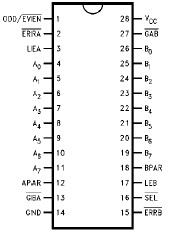
Pinout

  Connection Diagram


Specifications

Storage Temperature                                          -65 to +150
Ambient Temperature under Bias                        -55 to +125
Junction Temperature under Bias                        -55 to +150
VCC Pin Potential to Ground Pin                          -0.5V to +7.0V
Input Voltage (Note 3)                                          -0.5V to +7.0V
Input Current (Note 3)                                   -30 mA to +5.0 mA
Voltage Applied to Output
in HIGH State (with VCC = 0V)
Standard Output                                                     -0.5V to VCC
3-STATE Output                                                    -0.5V to +5.5V
Current Applied to Output
in LOW State (Max)                             Twice the Rated IOL (mA)
ESD Last Passing Voltage (Min)                                        4000V


Description

The 74F899 is a 9-bit to 9-bit parity transceiver with transparent latches. The device can operate as a feed-through transceiver or it can generate/check parity from the 8-bit data busses in either direction. It has a guaranteed current sinking capability of 24 mA at the A-bus and 64 mA at the B-bus.

The 74F899 features independent latch enables for the A-to-B direction and the B-to-A direction, a select pin for ODD/EVEN parity, and separate error signal output pins for checking parity.


Customers Who Bought This Item Also Bought

Margin,quality,low-cost products with low minimum orders. Secure your online payments with SeekIC Buyer Protection.
Optoelectronics
Memory Cards, Modules
Inductors, Coils, Chokes
Isolators
View more