Features: · High-speedÐgreater than a 30 MHz microinstruction rate· Three 4-bit registers· 16 instructions for register manipulation· Two separate output ports, one transparent· Relative addressing capability· TRI-STATE Outputs· Optional pre- or post- arithmetic· Expandable in multiples of fou...
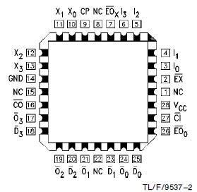
54F407: Features: · High-speedÐgreater than a 30 MHz microinstruction rate· Three 4-bit registers· 16 instructions for register manipulation· Two separate output ports, one transparent· Relative address...
SeekIC Buyer Protection PLUS - newly updated for 2013!
268 Transactions
All payment methods are secure and covered by SeekIC Buyer Protection PLUS.
Features: · Separate input and output clocks· Parallel input and output· Expandable without extern...
Storage Temperature -65 to a150
Ambient Temperature under Bias -55 to a125
Junction Temperature under Bias -55 to a175
VCC Pin Potential toGround Pin -0.5V to a7.0V
Input Voltage (Note 2) -0.5V to a7.0V
Input Current (Note 2) -30 mA to +5.0 mA
Voltage Applied to Output
in HIGH State (with VCC e 0V)
Standard Output -0.5V to VCC
TRI-STATE Output -0.5V to a5.5V
Current Applied to Output
in LOW State (Max) twice the rated IOL (mA)
Note 1: Absolute maximum ratings are values beyond which the device may be damaged or have its useful life impaired. Functional operation under these conditions is not implied.
Note 2: Either voltage limit or current limit is sufficient to protect inputs.
The 54F407 Data Access Register (DAR) performs memory address arithmetic for RAM resident stack applications. It contains three 4-bit registers intended for Program Counter (R0), Stack Pointer (R1), and Operand Address (R2). The 54F407 implements 16 instructions which allow either pre- or post-decrement/increment and register-to-register transfer in a single clock cycle. It is expandable in 4-bit increments and can operate at a 30 MHz microinstruction rate on a 16-bit word. The TRI-STATEÉ outputs of 54F407 are provided for busoriented applications. The 'F407 is fully compatible with all TTL families.