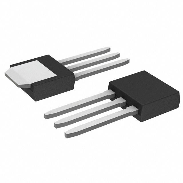
DescriptionThe 2SK423 is desined as toshiba field effect transistor silicon N channel MOS type for high speed switching applications and DC-DC converter and interface applications.2SK423 has four features. (1)Excellent switching times which means toff=20ns typ. (2)High forward transfer admittance ...
2SK423: DescriptionThe 2SK423 is desined as toshiba field effect transistor silicon N channel MOS type for high speed switching applications and DC-DC converter and interface applications.2SK423 has four fe...
SeekIC Buyer Protection PLUS - newly updated for 2013!
268 Transactions
All payment methods are secure and covered by SeekIC Buyer Protection PLUS.
The 2SK423 is desined as toshiba field effect transistor silicon N channel MOS type for high speed switching applications and DC-DC converter and interface applications.
2SK423 has four features. (1)Excellent switching times which means toff=20ns typ. (2)High forward transfer admittance which would be 150ms typ at Id=0.3A. (3)Low leakage current which means Igss=+/-100nA max at Vgs=+/-20V and Idss=1mA max at Vds=100V. (4)Exhancement mode which means Vth=1.5V to 3.5V at Id=1mA. Those are all the main features.
Some absolute maximum ratings of 2SK423 have been concluded into several points as follow. (1)Its drain-source voltage would be 100V. (2)Its gate-source voltage would be +/-20V. (3)Its drain current would be 0.5A for DC and would be 0.8A for pulse. (4)Its drain power dissipation would be 900mW. (5)Its channel temperature would be 150°C. (6)Its storage temperature range would be from -55°C to 150°C. It should be noted that stresses above those listed in absolute maximum ratings may cause permanent damage to device.
Also some electrical characteristics of 2SK423 are concluded as follow. (1)Its gate leakage current would be max +/-100nA. (2)Its drain cut-off current would be max 1.0mA. (3)Its drain-source breakdown voltage would be min 100V. (4)Its gate threshold voltage would be min 1.5V and max 3.5V. (5)Its forward transfer admittance would be min 50S and typ 150S. (6)Its drain to source ON resistance would be typ 2.4 and max 4.5. (7)Its drain to source ON voltage would be typ 2.5V and max 4.3V. (8)Its input capacitance would be typ 40pF and max 70pF. (9)Its reverse transfer capacitance would be typ 14pF and max 30pF. (10)Its output capacitance would be typ 50pF and max 80pF. (11)Its switching time rise time would be typ 10ns and max 20ns. (12)Its turn-on time would be typ 15ns and max 30ns. (13)Its fall time would be typ 13ns and max 25ns. (14)Its turn-off time would be typ 20ns and max 40ns. And so on. If you have any question or suggestion or want to know more information please contact us for details. Thank you!