Series: -
Transistor Type: -
Current - Collector (Ic) (Max): -
FET Feature: Logic Level Gate
Voltage - Collector Emitter Breakdown (Max): -
Vce Saturation (Max) @ Ib, Ic: -
Current - Collector Cutoff (Max): -
DC Current Gain (hFE) (Min) @ Ic, Vce: -
Frequency - Transition: -
FET Type: MOSFET P-Channel, Metal Oxide
Current - Continuous Drain (Id) @ 25° C: 16A
Drain to Source Voltage (Vdss): 100V
Packaging: Tube
Mounting Type: Through Hole
Power - Max: 60W
Gate Charge (Qg) @ Vgs: 48nC @ 10V
Vgs(th) (Max) @ Id: 2V @ 1mA
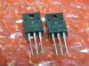
Package / Case: TO-220-3, Short Tab
Manufacturer: Toshiba
Input Capacitance (Ciss) @ Vds: 1100pF @ 10V
Rds On (Max) @ Id, Vgs: 210 mOhm @ 6A, 10V
Supplier Device Package: TO-220FL
DescriptionThe 2SJ412 is a kind of P-channel silicon MOS transistor.It is used for high speed,high current switching and DC-DC cinverter,relay drive and motor drive applications.It has some faetures as follows.(1) 4 V gate drive; (2) low drain-source on resistance; (3) high forward transfer admittance; (4) low leakage current; (5) enhancement-mode.
Then is absolute maximum ratings of 2SJ412 when TA is 25. (1): drain-source voltage(VDSS) is -100 V; (2): drain-gate voltage(VDGR) is -100 V; (3): gate-source voltage(VGSS) is ±20 V; (4): DC drain current(ID) is -16 A and pulse drain current(IPD) is -64 A; (5): drain power dissipation(PD) is 60 W; (6): single pulse avalanche energy(EAS) is 292 mJ; (7): avalanche current(IAR) is -16 A; (8): repetitive avalanche energy(EAR) is 6 mJ; (9): channel temperature(TCH) is 150; (10): storage temperature range is from -55 to 150.
What comes next is elecrtical characteristics of 2SJ412 at TA is 25.(1): the maximum gate leakage current is ±10 A at the condition of VGS is ±16 V and VDS is 0 V ; (2): the maximum drain cutoff current is -100 A when VDS is -100 V and VGS is 0 V; (3): the mithe minimum gate threshold voitage is -0.8 V and is -2.0 V for the maximum when VDS is -10 V and ID is -1 mA; (5): the typical forward transfer admittance is 7.7 S and is 4.5 S for the minimum at VDS is -10 V and ID is -6 A.
Parameters: | Technical/Catalog Information | 2SJ412 |
| Vendor | Toshiba |
| Category | Discrete Semiconductor Products |
| Mounting Type | Through Hole |
| FET Polarity | P-Channel |
| Drain to Source Voltage (Vdss) | 100V |
| Current - Continuous Drain (Id) @ 25° C | 16A |
| Rds On (Max) @ Id, Vgs | 210 mOhm @ 6A, 10V |
| Input Capacitance (Ciss) @ Vds | 1100pF @ 10V |
| Power - Max | 60W |
| Packaging | Tube |
| Gate Charge (Qg) @ Vgs | 48nC @ 10V |
| Package / Case | TO-220 |
| FET Feature | Logic Level Gate |
| Lead Free Status | Contains Lead |
| RoHS Status | RoHS Non-Compliant |
| Other Names | 2SJ412
2SJ412
|

 2SJ412 Data Sheet