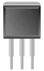
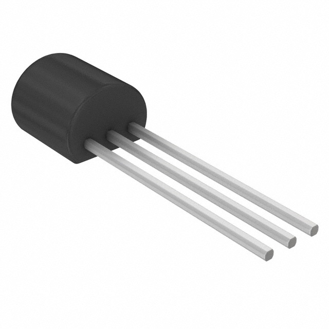
Features: SpecificationsDescription The 2N7002KG (190 mA, 60 V, RDS(ON) = 2 N-Ch Small Signal MOSFET with gate protection ) is under 2 kV ESD protected, with the lower On-resistance(2 ), low input capacitance(25 pF), low input and output leakage, fast switching performance(25 nS), low threshold(2V(Typ.)). And its weight is 0.07800g (Approximately), made in the code of K7K.
The 2N7002KG can be used in the areas of solid-state relays, drivers(Relays, Solenoids, Lamps Hammers, Display, Memories, Transistors, etc.), direct logic-level interface(TTL/CMOS), battery operated systems.Some parameters are got. VDS(Drain-Source Voltage)=60V, VGS(Gate-Source Voltage)=±20V, ID(Continuous Drain Current, Surface mounted on FR4 board.)=300mA(@TA=25°C)/190mA(@TA=100°C), IDM(Pulsed Drain Current, Pulse width limited by maximum junction temperature)=800, PD(Power Dissipation, Surface mounted on FR4 board)=0.35W(@TA=25°C)/0.14W(@TA=100°C), RJA(Thermal Resistance Junction-Ambient)=350°C/W, TJ, TSTG(Operating Junction and Storage Temperature)=-55 to +150 °C.And the electrical properties are V(BR)DSS(Drain-Source Breakdown Voltage, @ VGS = 0, ID = 10uA)=60V(min), V GS(th) (Gate-Threshold Voltage, @ VDS = VGS, ID = 250uA)=1.0(min)/2.5(max)V, gfs(Forward Transconductance, @ VDS = 10V, ID = 200 mA, for DESIGN AID ONLY, not subject to production testing)=100mS, IGSS(max)(Gate-Body Leakage Current)=±10 A(VDS = 0, VGS = ±20V)/±150nA(VDS = 0, VGS = ±10V)/±1000nA(VDS=0,VGS=±10V,TJ=85°C)/±100 nA(VDS = 0, VGS = ±5V), I DSS(max) (Zero Gate Voltage Drain Current)=10nA(VDS = 50, VGS = 0)/100nA(VDS = 50V, VGS=0, TJ=85°C)/1A (VDS = 60V, VGS = 0)/500A(VDS=60V, VGS=0, TJ=125°C), ID(min)(ON)(On-State Drain Current, For DESIGN AID ONLY, not subject to production testing)=800mA(VGS = 10V, VDS = 7.5V)/500mA(VGS = 4.5V, VDS = 10V), rDS(ON)(MIN)(Drain-Source On-Resistance, For DESIGN AID ONLY, not subject to production testing)=2(VGS = 10V, IDS = 500mA)/4(VGS = 4.5V, IDS = 200mA), V DS(ON) (Diode Forward Voltage )1.3V(max)(IS = 200mA, VGS =0). For the dynamic(For DESIGN AID ONLY, not subject to production testing), Qg(Total Gate Charge)=0.4(typ)nC/0.6(max)nC(@ VDS=10V,VGS=4.5V,ID=250mA), (typ.)Ciss(input Capacitance)/Coss(Output Capacitance)/Crss(Reverse Transfer Capacitance)=30pF/6pF/2.5pF(all @ VDS=25V, VGS=0V, f=1MHz). For Switching(For DESIGN AID ONLY, not subject to production testing; pulse test: PW 300s duty cycle 2% ), (min.)t(ON) (Turn-On Time)/t(OFF) (Turn-Off Time)=25nS/35n (VDD=30V,RL=150,ID= 200mA,VGEN=10V,RG=10).

 2N7002KG Data Sheet


