Features: · Output Stages Operate Antiphase Reducing Input and Output Capacitance Requirements and Power Sup ply Induced Noise
· Dual Input Supply Capability for Load Sharing
· 5-Bit AMD (Hammer) CPU VID Code: VOUT = 0.8V to 1.55V
· ±1% Output Voltage Accuracy
· True Remote Sensing Differential Amplifier
· Power Good Output Voltage Monitor
· Supports Active Voltage Positioning
· Current Mode Control Ensures Current Sharing
· OPTI-LOOP® Compensation Minimizes COUT
· Three Operational Modes: PWM, Burst and Cycle Skip
· Programmable Fixed Frequency: 150kHz to 300kHz
· Wide VIN Range: 4V to 36V Operation
· Adjustable Soft-Start Current Ramping
· Internal Current Foldback and Short-Circuit Shutdown
· Overvoltage Soft Latch Eliminates Nuisance Trips
· Available in 36-Lead Narrow (0.209) SSOP Package
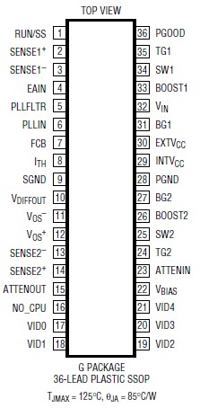
Pinout Specifications
Input Supply Voltage (VIN).............................36V to 0.3V
Topside Driver Voltages (BOOST1,2) .............42V to 0.3V
Switch Voltage (SW1, 2) .................................36V to 5 V
SENSE1+, SENSE2 +, SENSE1,
SENSE2 Voltages .......................... (1.1)INTVCC to 0.3V
EAIN, VOS +, VOS ,
EXTVCC, INTVCC, RUN/SS,
VBIAS, ATTENIN, ATTENOUT, PGOOD, NO_CPU,
VID0VID4, Voltages ......................................7V to 0.3V
Boosted Driver Voltage (BOOST-SW) .............7V to 0.3V
PLLFLTR, PLLIN, VDIFFOUT,
FCB Voltages ........................................ INTVCC to 0.3V
ITH Voltage ................................................2.7V to 0.3V
Peak Output Current <1ms(TG1, 2, BG1, 2) ............... 3A
INTVCC RMS Output Current .................................. 50mA
Operating Ambient Temperature Range
(Note 2) .................................................... 40 to 85
Junction Temperature (Note 3) ............................. 125
Storage Temperature Range .................. 65 to 150
Lead Temperature (Soldering, 10 sec)................... 300
DescriptionThe LTC®3719 is a 2-phase, VID programmable, synchronous step-down switching regulator controller that drives two N-channel external power MOSFET stages in a fixed frequency architecture. The LTC®3719 drives its two output stages out of phase at frequencies up to 300kHz to minimize the RMS ripple currents in both input and output capacitors. The 2-phase technique effectively multiplies the fundamental frequency by two, improving transient response while operating each channel at an optimum frequency for efficiency. Thermal design is also simplified.
An operating mode select pin (FCB) can be used to regulate a secondary winding or select among three modes including Burst Mode® operation for highest efficiency. An internal differential amplifier provides true remote sensing of the regulated supply's positive and negative output terminals as required in high current applications.
The RUN/SS pin provides soft-start and optional timed, short-circuit shutdown. Current foldback limits MOSFET dissipation during short-circuit conditions when the overcurrent latchoff is disabled. OPTI-LOOP compensation allows the transient response to be optimized for a wide range of output capacitors and ESR values.

 24019 Data Sheet


