Pinout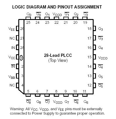 Specifications
|
Symbol |
Parameter |
Condition 1 |
Condition 2 |
Rating |
Unit |
|
VCC |
PECL Mode Power Supply |
VEE = 0 V |
|
8 to 0 |
V |
|
VEE |
NECL Mode Power Supply |
VCC = 0 V |
|
-8 to 0 |
V |
|
VI |
PECL Mode Input Voltage
NECL Mode Input Voltage |
VEE = 0 V
VCC = 0 V |
VI � VCC
VI � VEE |
6 to 0
6 to 0 |
V
V |
|
Iout |
Output Current |
Continuous
Surge |
|
50
100 |
mA
mA |
|
IBB |
VBB Sink/Source |
|
|
± 0.5 |
mA |
|
TA |
Operating Temperature Range |
|
|
-40 to +85 |
°C |
|
Tstg |
Storage Temperature Range |
|
|
-65 to +150 |
°C |
|
�JA |
Thermal Resistance (Junction-to-Ambient) |
0 LFPM
500 LFPM |
28 PLCC
28 PLCC |
80
55 |
°C/W
°C/W |
|
�JC |
Thermal Resistance (Junction-to-Case) |
std bd |
28 PLCC |
22 to 26 ± 5% |
°C/W |
|
Tsol |
Wave Solder |
< 2 to 3 sec @ 248°C |
|
265 |
°C |
DescriptionThe MC100LVE111 is a low skew 1-to-9 differential driver, designed with clock distribution in mind. The MC100LVE111's function and performance are similar to the popular MC100E111, with the added feature of low voltage operation. It accepts one signal input, which can be either differential or single-ended if the VBB output is used. The signal is fanned out to 9 identical differential outputs.
The LVE111 is specifically designed, modeled and produced with low skew as the key goal. Optimal design and layout serve to minimize gate to gate skew within a device, and empirical modeling is used to determine process control limits that ensure consistent tpd distributions from lot to lot.
The net result is a dependable, guaranteed low skew device. To ensure that the tight skew specification is met it is necessary that both sides of the differential output are terminated into 50 W, even if only one side is being used. In most applications, all nine differential pairs will be used and therefore terminated. In the case where fewer than nine pairs are used, it is necessary to terminate at least the output pairs on the same package side as the pair(s) being used on that side, in order to maintain minimum skew. Failure to do this will result in small degradations of propagation delay (on the order of 1020 ps) of the output(s) being used which, while not being catastrophic to most designs, will mean a loss of skew margin. The MC100LVE111, as with most other ECL devices, can be operated from a positive VCC supply in PECL mode. This allows the LVE111 to be used for high performance clock distribution in +3.3 V systems. Designers can take advantage of the LVE111's performance to distribute low skew clocks across the backplane or the board. In a PECL environment, series or Thevenin line terminations are typically used as they require no additional power supplies. For systems incorporating GTL, parallel termination offers the lowest power by taking advantage of the 1.2 V supply as a terminating voltage. For more information on using PECL, designers should refer to Application Note AN1406/D. The VBB pin, an internally generated voltage supply, is available to this device only. For single-ended input conditions, the unused differential input is connected to VBB as a switching reference voltage. VBB may also rebias AC coupled inputs. When used, decouple VBB and VCC via a 0.01 �F capacitor and limit current sourcing or sinking to 0.5 mA. When not used, VBB should be left open.

 200807101831199535 Data Sheet