Circuit Diagram
Index 2208
12V Soft start fixed voltage power supply circuit diagram
Published:2011/3/21 22:48:00 Author:Rebekka | Keyword: Soft start, fixed voltage power supply
View full Circuit Diagram | Comments | Reading(1116)
Crystal triode IMH1A、IMH2A、IMH9A inside circuit diagram
Published:2011/3/24 0:57:00 Author:Ecco | Keyword: Crystal triode
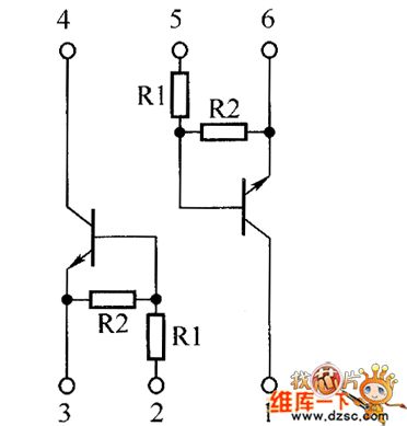
Crystal triode IMH1A、IMH2A、IMH9A inside circuit diagram is as below:
(View)
View full Circuit Diagram | Comments | Reading(445)
Internal resistance of power source measuring and test circuit diagram
Published:2011/3/20 22:56:00 Author:Ecco | Keyword: Internal resistance, power source

Internal resistance of power source measuring and test circuit diagram is as below:
(View)
View full Circuit Diagram | Comments | Reading(512)
Relay measurment circuit diagram
Published:2011/3/20 22:56:00 Author:Ecco | Keyword: Relay measurment
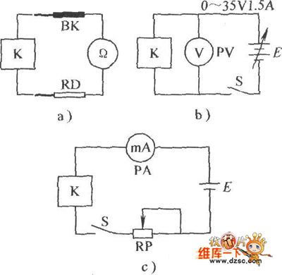
Relay measurment circuit diagram is as below:
(View)
View full Circuit Diagram | Comments | Reading(560)
Crystal triode IMH5A、IMH6A inside circuit diagram
Published:2011/3/20 22:56:00 Author:Ecco | Keyword: Crystal triode
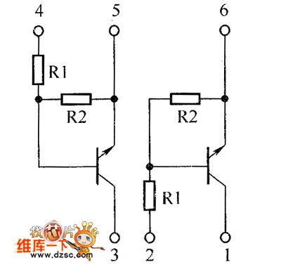
Crystal triode IMH5A、IMH6A inside circuit diagram is as below:
(View)
View full Circuit Diagram | Comments | Reading(383)
Intelligent pressure measurement and control circuit diagram
Published:2011/3/20 22:56:00 Author:Ecco | Keyword: Intelligent pressure measurement and control

Intelligent pressure measurement and control circuit diagram is as below:
(View)
View full Circuit Diagram | Comments | Reading(1248)
Switching regulator supply circuit diagram with three terminal regulator
Published:2011/3/29 3:26:00 Author:Ecco | Keyword: three terminal regulator, Switching regulator supply

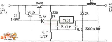
As shown in chart, the switching regulator supply circuit is made from three terminal regulator, and the working principle can be understood by the equivalent circuit diagram. For some reason, the output voltage V0 declined slightly, its separate pressure V3 in R5 and R6 fall subsequently, and magnified by VT3, the Ic3 decreases, and Ic2 increases, namely the current flowed through R1 and VD1 increases, V1 drops, V4, Ic1 increase, V2 rises, and cause V3 down... This process is a positive feedback chain reaction, and the last result is that VT1, VT2 are conducted strongly, VT3 stops working, IC1 charges for L1, C1, and Vo rises, then causes a series of positive feedback chain reaction. After a short time, Vo's rising results in the conduction of VT3, the deadline of VT1, VT2. The current stored on L1 released by load and diode VD2, which resulting in V4 dropping to 0. Of course Vo also slowly down until the second flip, namely completes self-excited oscillation of a cycle. The whole circuit works in the cycle of switching state.
(View)
View full Circuit Diagram | Comments | Reading(614)
Venturi Filter circuit diagram
Published:2011/3/20 22:56:00 Author:Ecco | Keyword: Venturi Filter
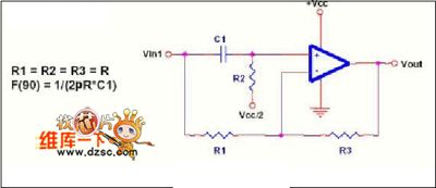
Venturi Filter circuit diagram is as below:
(View)
View full Circuit Diagram | Comments | Reading(517)
LED digital tube static display drive circuit diagram
Published:2011/3/23 4:46:00 Author:Nicole | Keyword: LED digital tube, display drive
View full Circuit Diagram | Comments | Reading(612)
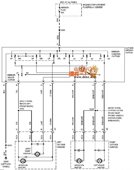
Cadillac deville electric rearview mirror circuit diagram
Published:2011/3/24 4:43:00 Author:Nicole | Keyword: Cadillac, electric rearview mirror
View full Circuit Diagram | Comments | Reading(468)
Efficient Sine Inverter Circuit Diagram
Published:2011/3/21 1:47:00 Author:Rebrecca | Keyword: Sine Inverter

Efficient Sine Inverter Circuit Diagram is shown as below.
(View)
View full Circuit Diagram | Comments | Reading(1004)
Fahrenheit scale circuit diagram
Published:2011/3/20 22:56:00 Author:Ecco | Keyword: Fahrenheit scale

Fahrenheit scale circuit diagram is as below:
(View)
View full Circuit Diagram | Comments | Reading(804)
ne5532 preamplifier circuit diagram
Published:2011/3/20 22:56:00 Author:Ecco | Keyword: preamplifier

ne5532 preamplifier circuit diagram is as below:
(View)
View full Circuit Diagram | Comments | Reading(6691)
ne5532 Low noise amplifier circuit diagram 2
Published:2011/3/20 22:54:00 Author:Ecco | Keyword: Low noise amplifier
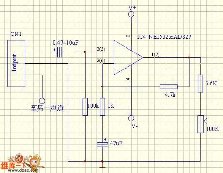
ne5532 Low noise amplifier circuit diagram 2 is below:
(View)
View full Circuit Diagram | Comments | Reading(3443)
Alarm control keyboard circuit diagram
Published:2011/3/20 22:54:00 Author:Ecco | Keyword: Alarm, control keyboard
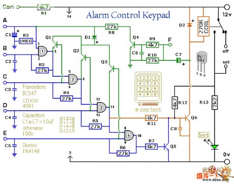
Alarm control keyboard circuit diagram is as below:
(View)
View full Circuit Diagram | Comments | Reading(446)
ne5532 Low noise amplifier circuit diagram 1
Published:2011/3/20 22:54:00 Author:Ecco | Keyword: Low noise amplifier
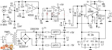
ne5532 Low noise amplifier circuit diagram 1is as below:
(View)
View full Circuit Diagram | Comments | Reading(7436)
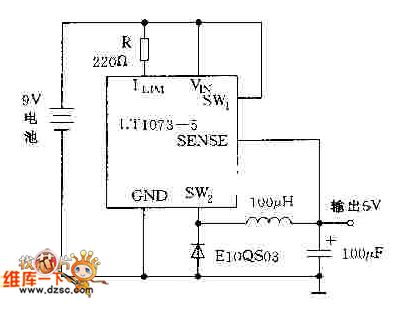
Step-down circuit diagram composed of LT1073
Published:2011/3/28 4:18:00 Author:Nicole | Keyword: Step-down
View full Circuit Diagram | Comments | Reading(817)
6B59 Drive LED display circuit diagram
Published:2011/3/20 22:54:00 Author:Ecco | Keyword: 6B59 Drive, LED display

6B59 Drive LED display circuit diagram is as below:
(View)
View full Circuit Diagram | Comments | Reading(531)
Resonator grid drive circuit diagram
Published:2011/3/28 3:57:00 Author:Nicole | Keyword: Resonator grid
View full Circuit Diagram | Comments | Reading(501)
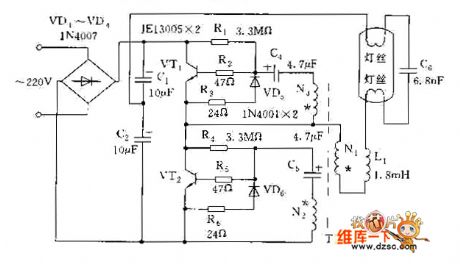
Serial electronic rectifier circuit diagram
Published:2011/3/28 4:03:00 Author:Nicole | Keyword: electronic rectifier
View full Circuit Diagram | Comments | Reading(407)
| Pages:2208/2234 At 2022012202220322042205220622072208220922102211221222132214221522162217221822192220Under 20 |
Circuit Categories
power supply circuit
Amplifier Circuit
Basic Circuit
LED and Light Circuit
Sensor Circuit
Signal Processing
Electrical Equipment Circuit
Control Circuit
Remote Control Circuit
A/D-D/A Converter Circuit
Audio Circuit
Measuring and Test Circuit
Communication Circuit
Computer-Related Circuit
555 Circuit
Automotive Circuit
Repairing Circuit


