
power supply circuit
Index 278
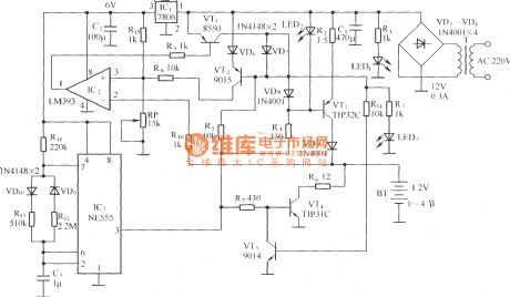
Ni-Cd battery constant source fast charger circuit (used as interphone)
Published:2011/4/1 3:09:00 Author:Nicole | Keyword: Ni-Cd battery, constant source, charger, interphone
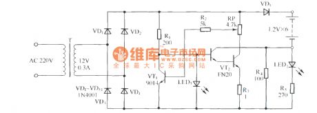
View full Circuit Diagram | Comments | Reading(590)
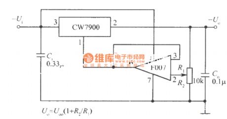
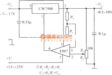
Fixed negative output voltage integrated regulated power supply
Published:2011/4/1 2:14:00 Author:Nicole | Keyword: negative output voltage, regulated power supply
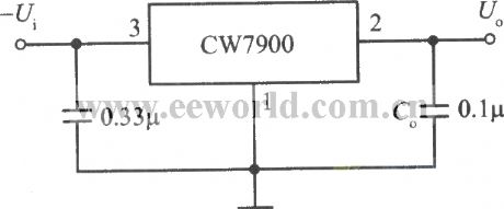
View full Circuit Diagram | Comments | Reading(459)
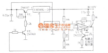
CW200 high output voltage integrated regulated power supply blocked up zero level
Published:2011/4/2 1:47:00 Author:Nicole | Keyword: zero level, high output voltage, regulated power supply
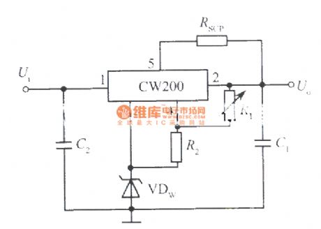
View full Circuit Diagram | Comments | Reading(442)
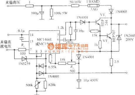
IOV regulated power supply circuit with network voltage between l20~250V
Published:2011/4/1 2:19:00 Author:Nicole | Keyword: IOV, regulated power supply, network voltage
View full Circuit Diagram | Comments | Reading(890)
Highly cost effective Ni-Cd battery charge circuit
Published:2011/4/1 2:07:00 Author:Nicole | Keyword: Ni-Cd battery, charge
View full Circuit Diagram | Comments | Reading(540)
High efficient sine inverter circuit
Published:2011/4/1 2:22:00 Author:Nicole | Keyword: sine inverter
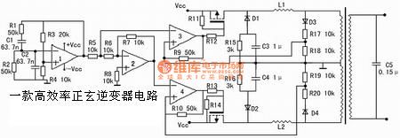
View full Circuit Diagram | Comments | Reading(688)
Heating blanket thermostat circuit diagram with temperature-controlled
Published:2011/4/1 2:48:00 Author:Nicole | Keyword: heating blanket, thermostat, temperature-controlled
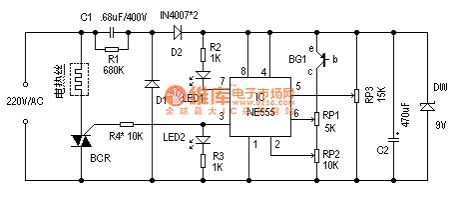
View full Circuit Diagram | Comments | Reading(2993)
Adjustable output integrated regulated power supply circuit 1
Published:2011/4/1 2:52:00 Author:Nicole | Keyword: regulated power supply
View full Circuit Diagram | Comments | Reading(500)
Adjustable output integrated regulated power supply circuit 2
Published:2011/4/1 2:52:00 Author:Nicole | Keyword: regulated power supply
View full Circuit Diagram | Comments | Reading(579)
Adjustable high voltage regulated power supply 1
Published:2011/4/1 2:54:00 Author:Nicole | Keyword: regulated power supply
View full Circuit Diagram | Comments | Reading(653)
Adjustable high voltage regulated power supply 2
Published:2011/4/1 2:54:00 Author:Nicole | Keyword: regulated power supply
View full Circuit Diagram | Comments | Reading(1781)
DVD-8829 switch power supply circuit
Published:2011/3/27 21:47:00 Author:may | Keyword: switch power supply
DVD-8829 switch power supply circuit is shown in the diagram:
(View)
View full Circuit Diagram | Comments | Reading(1007)
Highly-efficient step-up power supply circuit diagram composed of MAX632
Published:2011/3/23 3:01:00 Author:Nicole | Keyword: step-up power supply

As shown, this is the highly-efficient step-up power supply circuit diagram composed of MAX632. MAX6a is a high efficiency, few external components, low-power integrated switching regulator. Since switching power transistor and freewheeling diode has been integrated inside the chip, the MAX632 only need a energy storage inductor and a filter capacitor externally, it can easily form a Boost power circuit. The input voltage is range from +1.5 V to +12 V.
(View)
View full Circuit Diagram | Comments | Reading(1714)
200W voltage inverter circuit diagram
Published:2011/3/23 3:51:00 Author:Nicole | Keyword: 200W voltage inverter

View full Circuit Diagram | Comments | Reading(2673)
About high voltage follow circuit diagram
Published:2011/3/24 4:34:00 Author:Nicole | Keyword: high voltage follow

View full Circuit Diagram | Comments | Reading(594)
5W switching power supply circuit diagram
Published:2011/3/23 2:04:00 Author:Nicole | Keyword: 5W switching power supply

View full Circuit Diagram | Comments | Reading(2222)
60W switching power supply circuit diagram composed of UC3844
Published:2011/3/23 2:05:00 Author:Nicole | Keyword: 60W switching power supply

View full Circuit Diagram | Comments | Reading(7200)
Single-ended forward transform switching power supply circuit diagram
Published:2011/3/29 2:14:00 Author:Nicole | Keyword: Single-ended forward transform, switching power supply

The figure is a practical circuit of single-ended forward transform switching power supply. As using optocoupler in feedback loop, so the input and output have good isolation effect. The output voltage is 5V, output current is 10A. When connected to the power supply, it will output 300V DC voltage through VD1, L1, C1 rectifier filter, added to the switch VTl directly, and give the control circuit a working voltage to make it works.
During the switch VTl turns on, the secondary winding N2 of transformer T can obtain energy. The polarity make the rectifier diode VD3 conduction, and transfer to the load through L2, freewheeling diode VD4 is off. When VTl cuts off, storage inductor L2 releases energy, and the polarity in the two ends of L2 change, VD4 turns on, VD3 cuts off, L2 continues to provide energy to the load through VD4.
When the output voltage Uo rises for some reasons, the current of VT4, VT5 increases. The current is coupled to VT2 through optocoupler VT3, the resistance of VT2 decreased, then the base potential of control switch VTl decreases, the duty cycle of VTl decreases, Uo declines. Conversely, when Uo declines, to adjust in the opposite direction according to the above process, then it rebounded, so as to maintain Uo stable.
(View)
View full Circuit Diagram | Comments | Reading(1505)
Half-bridge converter power supply circuit diagram composed of two capacitors and high voltage transistors
Published:2011/3/29 1:26:00 Author:Nicole | Keyword: half-bridge converter, power supply, capacitor, transistor

In the high voltage switching power supply, the high Power Output always use half-bridge converter circuit. The figure as below, it is composed of two capacitors and two high voltage transistors. When two transistors cut off, if the capacity of two capacitors are equal and circuit symmetrical, then the voltage of point A is half of the input voltage. When VTl turns on, capacitor C01 will discharge through VTl, transformer primary winding N1; at the same time, capacitor C02 will charge through input power, VTl and primary winding N1 of T1. The potential of mid-point A will be decreased exponentially during the charge and discharge process. When VTl turns off, the potential of point A is (1 / 2) Ui-ΔUi, and the two transistors are all off. Collector to emitter voltage of two capacitors and two transistors is equal essentially, are all close to half of the input supply voltage. On the contrary, VT2 turns on, C02 discharges, C0l charges, the potential of point A will increase to (1 / 2) Ui + ΔUi, namely the potential of point A will be in the (1 / 2) Ui and index changed with the amplitude of ± △ U. Thus, in the half bridge circuit, the transformer primary winding always has current flowing in the whole cycle, the core is fully utilized.
(View)
View full Circuit Diagram | Comments | Reading(1802)
Boost output circuit diagram with low power dissipation
Published:2011/3/28 21:12:00 Author:Nicole | Keyword: boost output

VT3 is switching regulator; regulator tube VD2 can change potential; VT4 is inverting isolation amplifier; VT4 and its load 33kΩ resistor divide Ui. The two voltage supply for pulse generator circuit. Pulse generator circuit is composed of transformer T and VT1, VT2. This is a non-symmetric self-excited multivibrator of transformer feedback. The power supply of VTl is from 33kΩ resistor, and the current of resistance depends on VT4, VT1, VT2 have different supply voltage, the amplitude of each half weeks of oscillation is proportional changed, the width is inversely proportional changed, the on/off time of VT3 is controled. When the output voltage increases, the differential pair VT6 current of error amplifier increases, VT5 current decreases, the collector potential rises, VT4 current increases, the voltage of 33kΩ resistor voltage drop increases, VT1 supply voltage increases, shortened the on time, shortened the on time of switch VT3. According to the expression of boost output voltage: we can see, the output voltage Uo down to achieve voltage regulation. Conversely, when the output voltage drops, according to the above process to adjust on the opposite, to rise the output voltage, maintaining the output voltage stable. The input voltage is 12 ~ 28V, then the output voltage can be stable for the 30V, maximum output power is 60W, efficiency is 89.4% to 94.7%, instability is ± 0.33%, the output voltage ripple factor is 0.02%, operating frequency is 10kHz.
(View)
View full Circuit Diagram | Comments | Reading(562)
| Pages:278/291 At 20261262263264265266267268269270271272273274275276277278279280Under 20 |
Circuit Categories
power supply circuit
Amplifier Circuit
Basic Circuit
LED and Light Circuit
Sensor Circuit
Signal Processing
Electrical Equipment Circuit
Control Circuit
Remote Control Circuit
A/D-D/A Converter Circuit
Audio Circuit
Measuring and Test Circuit
Communication Circuit
Computer-Related Circuit
555 Circuit
Automotive Circuit
Repairing Circuit