Index 95
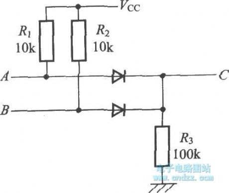
The OR circuit C = A + B composed of diode and resistor
Published:2011/12/5 1:53:00 Author:Ecco | Keyword: OR circuit , C = A + B , diode , resistor
View full Circuit Diagram | Comments | Reading(602)
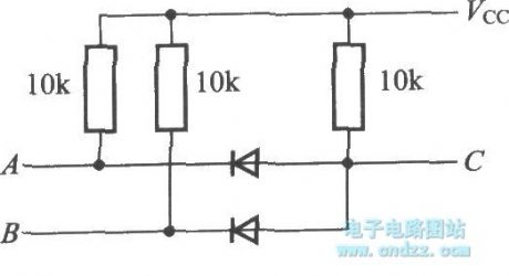
The AND circuit C = A · B composed of diodes and resistors
Published:2011/12/5 2:02:00 Author:Ecco | Keyword: AND circuit, C = A · B , diodes , resistors
View full Circuit Diagram | Comments | Reading(520)
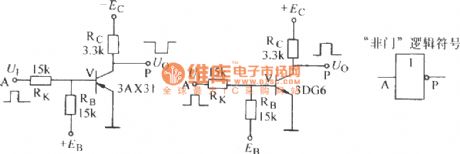
OR NOT gate circuit
Published:2011/12/5 2:07:00 Author:Ecco | Keyword: OR NOT gate

The transistor's emitter is used as the gate circuit of input gate, and it is known as the OR NOT gate, and it isshown in Figure a) . b)shows its logic symbols.
(View)
View full Circuit Diagram | Comments | Reading(887)
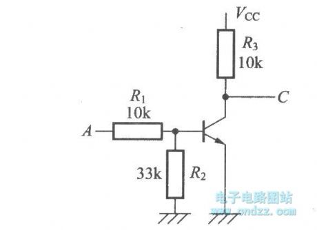
The NOT circuit using transistors
Published:2011/12/5 2:02:00 Author:Ecco | Keyword: NOT circuit , transistors
View full Circuit Diagram | Comments | Reading(534)
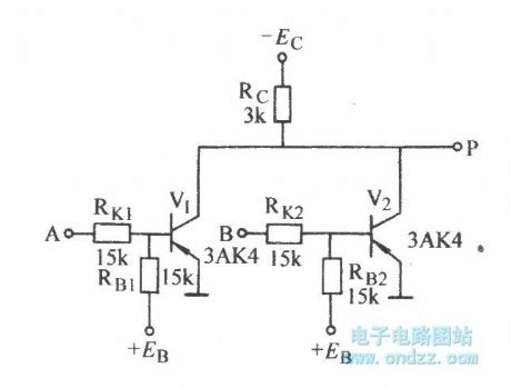
The transistor NOR gate circuit with two input ends
Published:2011/12/5 2:33:00 Author:Ecco | Keyword: transistor , NOR gate , two input ends
View full Circuit Diagram | Comments | Reading(980)
The transistor NOR gate circuit with resistance on two input ends
Published:2011/12/5 2:32:00 Author:Ecco | Keyword: transistor , NOR gate , resistance , two input ends
View full Circuit Diagram | Comments | Reading(598)
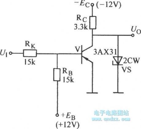
The NOT gate circuit clamping by Zener diode
Published:2011/12/5 2:30:00 Author:Ecco | Keyword: NOT gate, clamping, Zener diode
View full Circuit Diagram | Comments | Reading(1223)
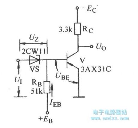
Zener diode threshold NOT gate circuit
Published:2011/12/5 2:28:00 Author:Ecco | Keyword: Zener diode , threshold , NOT gate
View full Circuit Diagram | Comments | Reading(1001)
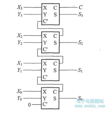
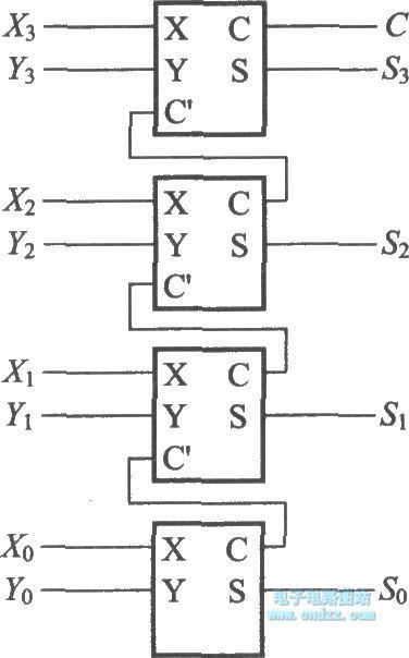
4-bit addition operation circuit using full adder
Published:2011/12/5 2:17:00 Author:Ecco | Keyword: 4-bit , addition operation , full adder
View full Circuit Diagram | Comments | Reading(1162)
4-bit addition operation circuit using half adder and full adder
Published:2011/12/5 2:21:00 Author:Ecco | Keyword: 4-bit , addition operation , half adder , full adder
View full Circuit Diagram | Comments | Reading(2480)
NOT gate circuit
Published:2011/12/5 2:12:00 Author:Ecco | Keyword: NOT gate
View full Circuit Diagram | Comments | Reading(803)
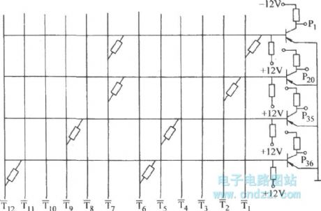
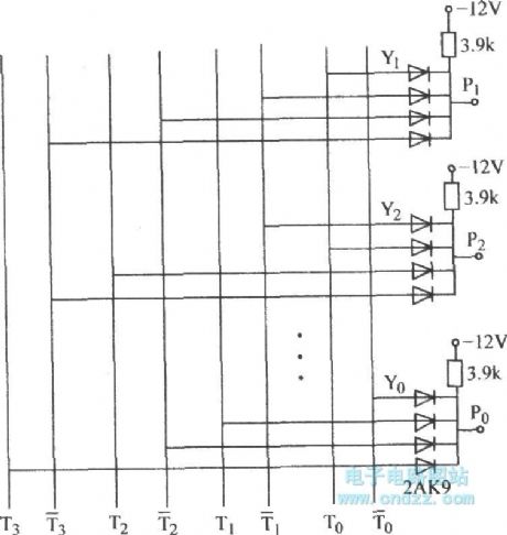
Diode AND gate decoder circuit (1)
Published:2011/12/5 2:23:00 Author:Ecco | Keyword: Diode , AND gate, decoder
View full Circuit Diagram | Comments | Reading(923)
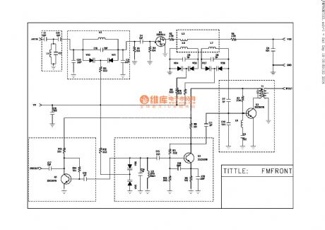
The classic tuner appreiation circuit diagram
Published:2011/12/9 1:21:00 Author:Ecco | Keyword: classic , tuner, appreiation
View full Circuit Diagram | Comments | Reading(528)
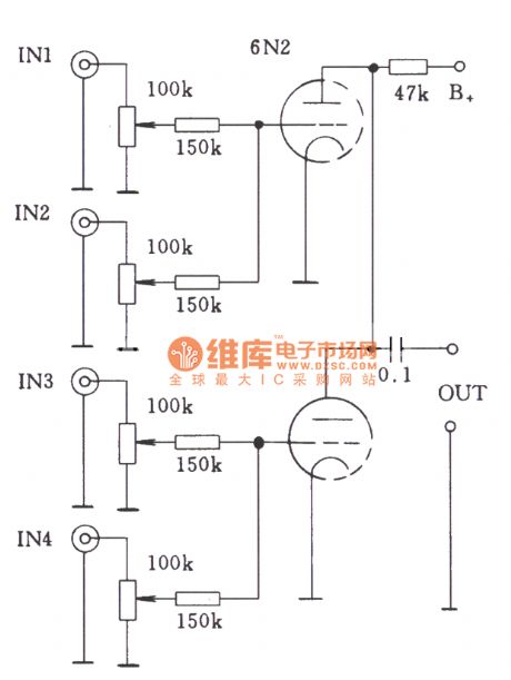
The single-stage multi- way resistor coupled - direct input mixed coupled tube circuit
Published:2011/12/9 1:19:00 Author:Ecco | Keyword: single-stage, multi- way resistor, coupled, direct input , mixed coupled, tube
View full Circuit Diagram | Comments | Reading(631)
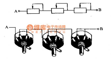
The precision potentiometer combination circuit adjusted in wide range
Published:2011/12/9 1:16:00 Author:Ecco | Keyword: precision, potentiometer, combination, adjusted , in wide range
View full Circuit Diagram | Comments | Reading(583)
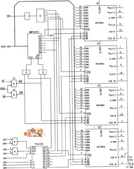
(ADC0840) Data acquisition system schematic diagram
Published:2011/12/9 0:59:00 Author:Ecco | Keyword: Data acquisition system
View full Circuit Diagram | Comments | Reading(1886)
ATX switching power auxiliary power supply maintenance circuit diagram
Published:2011/12/8 20:18:00 Author:Ecco | Keyword: ATX, switching power , auxiliary power supply, maintenance circuit
View full Circuit Diagram | Comments | Reading(2357)
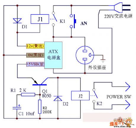
ATX power supply restructuring ( full outage with power off ) circuit diagram
Published:2011/12/8 20:15:00 Author:Ecco | Keyword: ATX, power supply , restructuring, full outage , power off
View full Circuit Diagram | Comments | Reading(1456)
Double-button touching light switching circuit ( 11 )
Published:2011/12/8 1:24:00 Author:Ecco | Keyword: Double-button , touching light , switching circuit
View full Circuit Diagram | Comments | Reading(516)
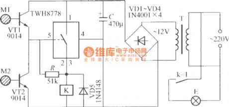
Double-button touching light switching circuit ( 10 )
Published:2011/12/8 1:23:00 Author:Ecco | Keyword: Double-button, touching light , switching circuit
In the circuit shown as the chart, K can be JZC-22F, DC12V small medium-power electromagnetic relay.
(View)
View full Circuit Diagram | Comments | Reading(522)
| Pages:95/471 At 2081828384858687888990919293949596979899100Under 20 |
Circuit Categories
power supply circuit
Amplifier Circuit
Basic Circuit
LED and Light Circuit
Sensor Circuit
Signal Processing
Electrical Equipment Circuit
Control Circuit
Remote Control Circuit
A/D-D/A Converter Circuit
Audio Circuit
Measuring and Test Circuit
Communication Circuit
Computer-Related Circuit
555 Circuit
Automotive Circuit
Repairing Circuit
